
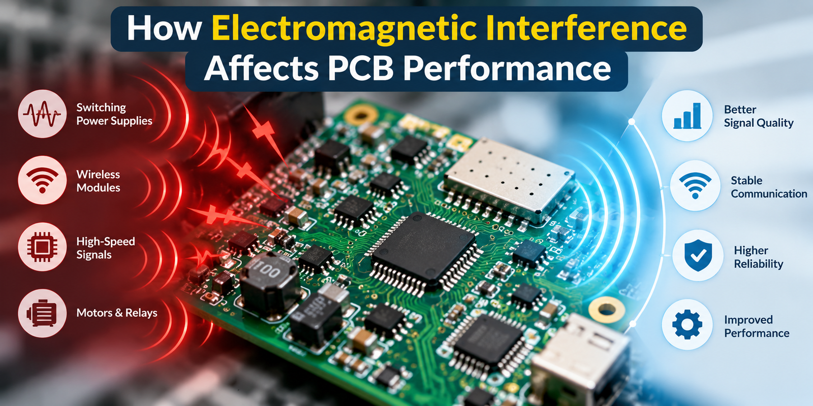
Electronic devices rely on printed circuit boards (PCBs) to connect components and process electrical signals. However, unwanted electromagnetic signals can interfere with these circuits.
This problem is known as electromagnetic interference (EMI). It can affect signal quality, communication, device performance, and overall reliability.
Therefore, understanding electromagnetic interference in PCB design can help hardware developers build more stable and reliable electronic products.
What Is Electromagnetic Interference?
Electromagnetic interference occurs when unwanted electrical or electromagnetic signals affect the normal operation of an electronic circuit.
A PCB can both create and receive electromagnetic noise. High-speed signals, power circuits, motors, wireless modules, and switching components can all generate interference.
For example, an IoT device may contain a processor, wireless module, sensors, and power circuits on the same PCB. Poor layout can allow noise from one circuit to affect another.
How Does EMI Affect PCB Performance?
EMI can create several problems in electronic devices.
1. Signal Quality Problems
Unwanted electrical noise can change the shape or quality of a signal.
This can cause communication errors, incorrect sensor readings, or unstable circuit operation.
High-speed circuits need extra attention because they can react more strongly to noise and signal distortion.
2. Communication Errors
Many PCBs use communication interfaces such as Wi-Fi, Bluetooth, USB, Ethernet, or other high-speed connections.
EMI can interfere with these signals and cause:
- Data errors
- Connection drops
- Slow communication
- Unstable device operation
For connected devices, these problems can reduce overall system reliability.
3. Sensor Interference
Sensors often detect small electrical changes. Strong electromagnetic noise can affect these signals and produce incorrect readings.
This issue can become important in medical equipment, industrial systems, IoT devices, and measurement equipment.
4. Reduced Device Reliability
Continuous electromagnetic noise can make electronic circuits behave unpredictably.
A device may restart, lose communication, produce incorrect outputs, or fail to perform as expected.
Therefore, engineers should consider EMI during the PCB design stage.
Common Sources of EMI
Several parts of an electronic system can generate electromagnetic interference.
High-Speed Signals
Fast-changing digital signals can create electromagnetic noise. Poor trace routing can make this problem worse.
Power Circuits
Switching regulators, power converters, and other power circuits can generate unwanted electrical noise.
Wireless Modules
Wi-Fi, Bluetooth, cellular, and other wireless systems produce radio-frequency signals. Designers must carefully separate these circuits from sensitive components.
Motors and Relays
Motors, relays, and other switching devices can create electrical noise when they turn on or off.
How to Reduce EMI in PCB Design
Designers can use several techniques to control electromagnetic interference.
1. Use a Proper Ground Plane
A good ground plane provides a low-impedance return path for electrical signals.
It can also help reduce unwanted noise and improve signal integrity.
2. Keep Traces Short
Long PCB traces can act like antennas and may pick up or radiate electromagnetic noise.
Designers should keep high-speed and sensitive signal traces as short as practical.
3. Separate Noisy and Sensitive Circuits
Power circuits and high-speed switching sections can generate significant noise.
Designers should keep these circuits away from sensitive analog or sensor circuits whenever possible.
4. Use Proper Trace Routing
Good trace routing can reduce unwanted coupling between signals.
Designers should carefully plan:
- Signal paths
- Ground connections
- Power traces
- High-speed interfaces
- Differential pairs
A well-planned layout can significantly improve PCB performance.
5. Add Filtering Components
Engineers can use capacitors, ferrite beads, common-mode chokes, and other filtering components to reduce unwanted noise.
The correct component depends on the type and frequency of the interference.
6. Consider Shielding
Some electronic circuits need additional protection from electromagnetic fields.
Designers can use shielding materials or shielded enclosures to reduce interference.
This approach can help protect sensitive circuits and wireless sections.
Why EMI Testing Matters
PCB designers should test prototypes before moving to large-scale production.
EMI testing can help identify unwanted emissions and interference problems early.
Testing can reveal issues related to:
- Signal routing
- Power supply noise
- Wireless circuits
- Grounding
- Shielding
- Component placement
Early testing can reduce redesign costs and improve product reliability.
EMI and PCB Performance
Good EMI control supports several areas of PCB performance.
It can help improve:
- Signal integrity
- Communication reliability
- Sensor accuracy
- Device stability
- Product reliability
- Electromagnetic compatibility
As electronic products become smaller and faster, EMI control becomes even more important.
Best Practices for Reducing EMI
Hardware developers can follow these simple practices:
- Plan the PCB layout before routing signals.
- Use proper grounding techniques.
- Keep high-speed traces short.
- Separate noisy and sensitive circuits.
- Place decoupling capacitors close to power pins.
- Use suitable filters where necessary.
- Consider shielding for sensitive circuits.
- Test the PCB before mass production.
These practices can help reduce electromagnetic interference and improve overall PCB performance.
Conclusion
Electromagnetic interference in PCB design can affect signal quality, communication, sensor accuracy, and device reliability.
However, careful PCB layout can reduce many EMI problems. Proper grounding, short signal paths, circuit separation, filtering, shielding, and testing all contribute to better EMI control.
By considering electromagnetic interference from the beginning of the design process, hardware developers can create PCBs that perform more reliably in real-world applications.
Frequently Asked Questions
What is electromagnetic interference in PCB?
Electromagnetic interference occurs when unwanted electromagnetic signals affect the normal operation of a PCB or electronic circuit.
What causes EMI in PCBs?
Common sources include high-speed signals, switching power circuits, wireless modules, motors, relays, and poorly designed signal paths.
How can PCB designers reduce EMI?
Designers can reduce EMI through proper grounding, short traces, circuit separation, filtering, shielding, and careful component placement.
Does EMI affect signal quality?
Yes. EMI can distort signals and cause communication errors, incorrect sensor readings, and unstable device operation.
Why should engineers test PCBs for EMI?
EMI testing helps engineers identify interference problems before mass production and improve the reliability of the final product.