
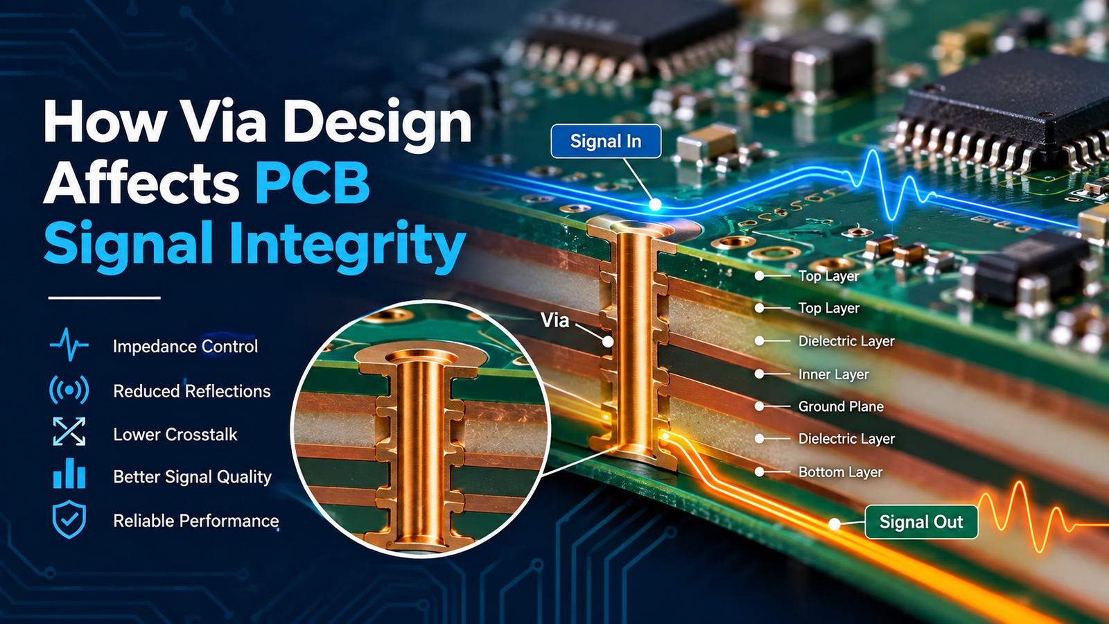
Vias are small structures, but they play a major role in PCB performance. They connect traces between different layers and help route signals through multilayer boards.
However, a poorly designed via can affect signal quality. This becomes more important as signal speeds increase.
Via design affects impedance, reflections, crosstalk, and signal loss. Therefore, engineers should consider vias during the early stages of high-speed PCB design.
In this article, we explain how via design affects PCB signal integrity and discuss practical ways to reduce common problems.
What Is a Via in PCB Design?
A via is a plated hole that connects copper layers in a printed circuit board.
For example, a signal may travel on the top layer and then move to an internal layer through a via.
A simple signal path can look like this:
Top Layer → Via → Inner Layer → Via → Bottom Layer
Vias make multilayer routing possible. They also help designers create compact and complex PCB layouts.
However, a via is not electrically invisible. At high frequencies, its structure can affect the signal.
Why Via Design Matters for Signal Integrity
Signal integrity describes how accurately a signal travels through a circuit.
A clean signal should reach its destination with minimal distortion. However, changes in the signal path can introduce unwanted electrical effects.
A via can create:
- Impedance changes
- Signal reflections
- Insertion loss
- Return loss
- Crosstalk
- Resonance
- Signal distortion
As signal speed increases, these effects can become more noticeable.
Therefore, designers should treat vias as part of the high-speed signal path rather than simple mechanical connections.
1. Via Size Can Affect Signal Behavior
The physical size of a via can influence its electrical characteristics.
A via contains several important dimensions, including:
- Drill diameter
- Pad diameter
- Antipad diameter
- Via barrel length
- Copper thickness
These dimensions affect the electromagnetic behavior of the signal.
For example, a larger via structure can introduce more parasitic capacitance. In contrast, a long via structure can increase parasitic inductance.
For this reason, designers should select via dimensions according to the signal requirements rather than using one standard size for every design.
2. Via Stubs Can Cause Signal Problems
A via stub is the unused portion of a via that extends beyond the signal layer connection.
Consider a signal that travels from the top layer to an inner layer. If the via continues through additional PCB layers, the unused section becomes a stub.
The structure can look like this:
Signal Layer
↓
Connection Point
↓
Unused Via Section
That unused section can behave like a transmission-line segment.
At high frequencies, the stub can cause reflections and resonance. As a result, the signal may experience distortion or loss.
Designers can reduce this problem by using techniques such as:
- Back drilling
- Blind vias
- Microvias
- Optimized layer stackups
The appropriate method depends on the PCB structure and manufacturing requirements.
3. Via Inductance Can Affect High-Speed Signals
A via contains a vertical conductive path. This path introduces parasitic inductance.
At lower frequencies, the effect may be small. However, high-speed signals can respond more strongly to this inductance.
Via inductance can affect:
- Signal transitions
- Power delivery
- Voltage levels
- Signal quality
Therefore, shorter current paths can help reduce unwanted inductive effects.
Designers should also avoid unnecessary vias in sensitive high-speed signal paths.
4. Vias Can Create Impedance Discontinuities
High-speed signals often use controlled impedance routing.
A trace may have a specific target impedance based on:
- Trace width
- Trace thickness
- Dielectric thickness
- PCB material
- Reference-plane structure
When the signal enters a via, its surrounding geometry changes.
Consequently, the via can create an impedance discontinuity.
This discontinuity can cause part of the signal to reflect toward the source.
A well-designed via transition should maintain a consistent signal environment as much as possible.
5. Via Placement Affects Crosstalk
Crosstalk occurs when energy from one signal path affects another nearby signal.
Via fields can contribute to this problem when several high-speed signals are routed close together.
For example:
High-Speed Signal Via
↓
Nearby Signal Via
The electromagnetic fields around these structures can interact.
As a result, unwanted noise can appear on nearby signal paths.
Designers can reduce this risk by:
- Increasing spacing between sensitive vias
- Separating noisy and sensitive signals
- Using appropriate ground vias
- Planning high-speed routing carefully
Good spacing becomes especially important when several high-speed interfaces share the same PCB area.
6. Ground Vias Can Improve Signal Integrity
Ground vias provide connections between PCB ground planes.
They can also support high-speed signal transitions by providing a nearby return-current path.
Consider a signal changing from one PCB layer to another.
The signal moves through a via. At the same time, its return current needs a suitable path.
If the return path becomes longer or interrupted, the signal transition can experience additional noise and electromagnetic interference.
A nearby ground via can help maintain a shorter return path.
This approach is particularly useful around:
- High-speed connectors
- Differential pairs
- RF circuits
- Layer transitions
- High-frequency interfaces
7. Differential Pair Vias Need Careful Design
Differential pairs carry two related signals.
Common examples include high-speed interfaces that use differential signaling.
The two traces should maintain a controlled relationship throughout the signal path.
However, poorly designed vias can disturb that relationship.
Differences in:
- Via position
- Pad size
- Trace length
- Ground-via placement
- Routing geometry
can create an imbalance between the two signals.
Therefore, both vias in a differential pair should use a consistent and symmetrical structure whenever possible.
This approach helps maintain the electrical balance of the pair.
8. Via Transitions Should Be as Short as Practical
Every layer transition changes the physical path of a signal.
An unnecessary transition can increase the overall electrical length and introduce another discontinuity.
For this reason, designers should avoid using unnecessary vias in sensitive signal paths.
A simpler path may look like:
Source → Trace → Receiver
A more complex path could look like:
Source → Trace → Via → Trace → Via → Trace → Receiver
The second path contains more transitions.
Therefore, reducing unnecessary layer changes can help simplify the signal path and reduce potential sources of signal degradation.
9. Back Drilling Can Reduce Via Stub Effects
Back drilling removes unused portions of a plated through-hole via.
The process creates a shorter effective via structure.
This approach can help reduce the effects of long via stubs in high-speed designs.
Back drilling can be useful in applications where signal integrity is particularly important.
However, it also adds manufacturing requirements.
Therefore, designers should consider back drilling when the signal-speed requirements justify the additional manufacturing process.
10. Microvias Can Support High-Density PCB Designs
Microvias are very small vias commonly used in high-density PCB structures.
They can connect adjacent layers without extending through the entire board.
This shorter structure can help reduce via-stub effects.
Microvias can also support:
- Compact routing
- High-density interconnects
- Smaller PCB designs
- Shorter layer transitions
However, microvias require suitable PCB manufacturing processes.
Therefore, designers should evaluate both electrical performance and manufacturing capability before selecting microvias.
Common Via Design Mistakes
Several via-related mistakes can affect PCB signal integrity.
Using Large Vias Without Considering Signal Requirements
Large vias can change the electrical environment around high-speed signals.
Leaving Long Via Stubs
Long stubs can create reflections and resonance at high frequencies.
Ignoring the Return Path
A signal transition without a suitable return path can increase noise and EMI.
Placing Signal Vias Too Close Together
Close spacing can increase coupling and crosstalk.
Using Asymmetrical Differential-Pair Vias
Unequal structures can disturb differential signaling.
Adding Unnecessary Layer Transitions
Extra vias can increase discontinuities in the signal path.
Careful planning can prevent many of these problems before the PCB reaches manufacturing.
Best Practices for Via Design
Designers can improve signal integrity by following these practices:
- Choose via dimensions based on the signal requirements.
- Keep high-speed via structures as short as practical.
- Minimize unnecessary via transitions.
- Reduce long via stubs where necessary.
- Provide a suitable return-current path.
- Place ground vias near high-speed signal transitions when appropriate.
- Maintain symmetry for differential-pair vias.
- Keep sensitive signal vias separated from noisy signals.
- Consider back drilling for high-speed applications.
- Use simulation when the design has demanding signal-integrity requirements.
How to Check Via Signal Integrity
Via performance can be evaluated during PCB development.
A typical design process can include:
Schematic → PCB Stackup → Via Design → Signal Integrity Analysis → Layout Review → Prototype Testing
Simulation can help identify:
- Impedance discontinuities
- Reflections
- Resonance
- Crosstalk
- Insertion loss
- Return loss
Testing can then verify the design under real operating conditions.
Early analysis is useful because designers can correct via problems before production.
Via Design for High-Speed PCB Applications
Via design becomes increasingly important as PCB operating frequencies and data rates increase.
Modern applications can include:
- Data communication equipment
- Networking hardware
- Computing systems
- Automotive electronics
- Industrial equipment
- IoT devices
- High-speed embedded systems
- RF and wireless hardware
Each application has different electrical and mechanical requirements.
As a result, there is no single via design that works for every PCB.
Designers should consider the signal speed, stackup, material, routing structure, manufacturing process, and required performance.
Conclusion
Vias are essential for multilayer PCB routing, but they can also affect signal integrity.
Via dimensions, stubs, inductance, impedance discontinuities, crosstalk, and return paths can all influence high-speed signal performance.
For this reason, via design should be part of the signal-integrity strategy from the beginning of PCB development.
A reliable approach combines careful via selection with controlled routing, proper grounding, suitable layer transitions, and signal-integrity analysis.
Ultimately, well-designed vias help create cleaner signal paths and more reliable high-speed PCBs.