
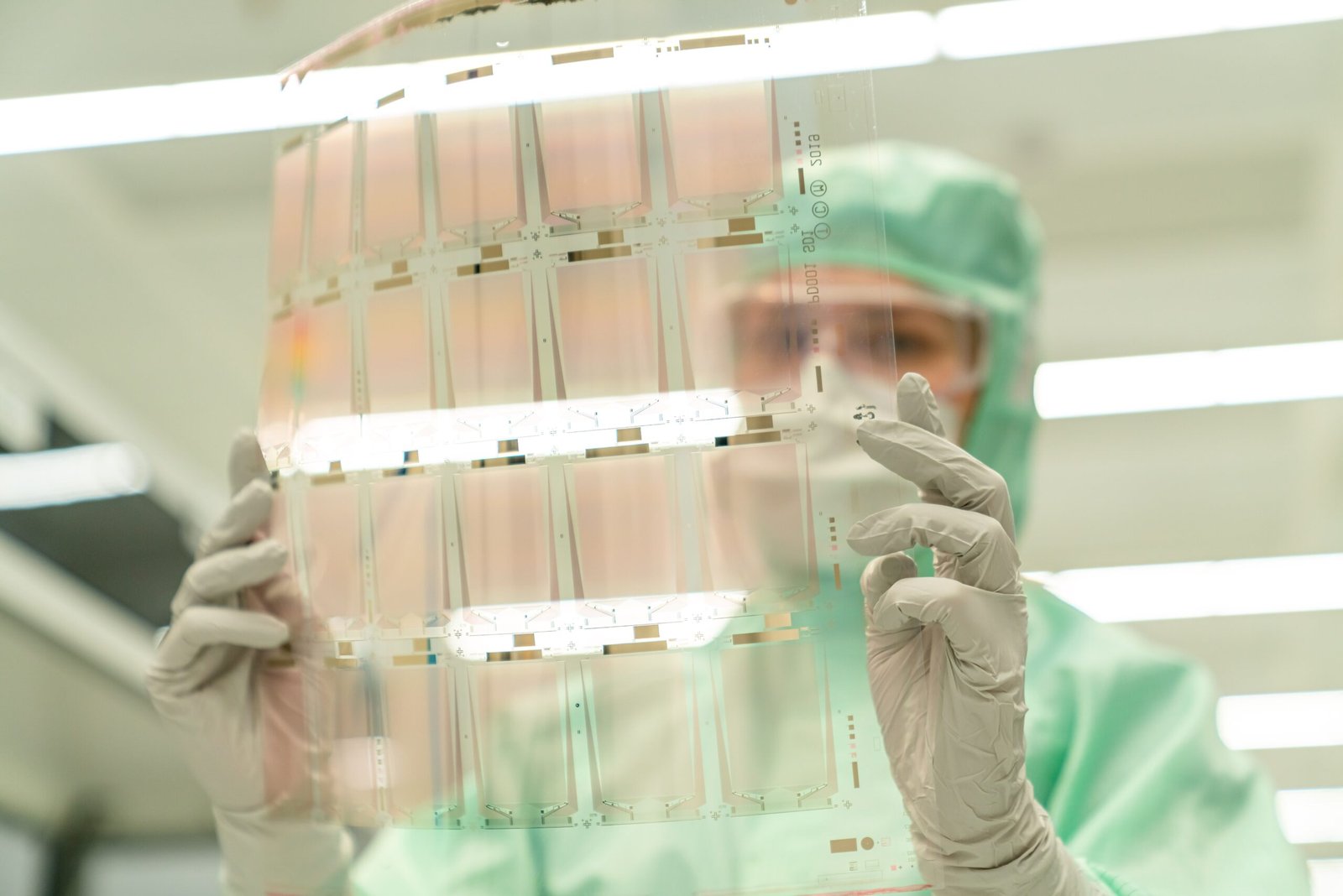
Wafer-level packaging is quietly replacing decades-old chip assembly methods. AI accelerators pushed the shift into overdrive. Traditional packaging simply cannot keep up with modern chip bandwidth demands. Wafer-level packaging solves that problem by rethinking how chips connect to everything around them. Here is how it works, and why it matters so much right now.
What Wafer-Level Packaging Actually Is
Wafer-level packaging completes the entire packaging process while chips are still on the wafer. Sometimes dies never even separate before packaging finishes. Other times, individual dies get rearranged into a reconstituted wafer first. Either way, the chip never touches a traditional substrate.
A redistribution layer, or RDL, does the real work here. It sits on top of the chip and fans signals out beyond the die’s physical edges. This eliminates the need for the organic or ceramic substrate that older packaging methods rely on. That single change unlocks dramatically tighter interconnect spacing.
Why Wafer-Level Packaging Beats Older Methods
Flip-chip BGA has dominated chip packaging for decades. It still works fine for many applications. But it hits a hard ceiling with modern AI accelerators.
The numbers make the gap obvious. Wafer-level packaging achieves interconnect pitches below 2 microns. Flip-chip BGA solder bumps sit between 100 and 150 microns. That is roughly fifty times denser. Consequently, wafer-level packaging can pack far more connections into the same physical space.
Bandwidth tells a similar story. Flip-chip BGA routes signals through a substrate first. That substrate becomes a bottleneck. Wafer-level packaging routes signals directly through the RDL instead. Data moves faster, with less energy wasted along the way.
The Bandwidth Wall Wafer-Level Packaging Solves
AI chips need bandwidth that old packaging methods simply cannot deliver. Neural network training is memory-bandwidth bound. That creates a real problem for flip-chip BGA designs.
Here is why. Placing memory beside a compute die in a flip-chip arrangement limits bandwidth to the number of connections along each die’s edge. That number scales with perimeter, not area. As chips grow larger, this becomes a serious constraint.
Wafer-level flips this equation. Vertical stacking through-silicon vias align directly with die-to-die connection counts. Bandwidth then scales with area instead of perimeter. For massive AI training accelerators, this difference decides whether a chip design even works.
Thermal Management Gets Built Into the Package
Modern AI processors run hot. Thermal design power in today’s accelerators often reaches 300 to 700 watts. That heat has to go somewhere, and traditional packaging was never built for loads this heavy.
Wafer-level packaging addresses this directly. Some designs integrate heat spreaders right into the package stack itself. The chip bonds to the heat spreader, and wiring grows across both the chip surface and the spreader’s structure. Therefore, heat moves out through the package rather than relying entirely on an external heat slug layered on top.
The One Real Weakness: Warpage
Wafer-packaging is not without tradeoffs. Warpage remains its biggest manufacturing challenge. When a reconstituted wafer contains embedded chips surrounded by molding compound, thermal expansion mismatches cause the whole wafer to bow during processing.
That bowing directly hurts yield, especially on large-format AI accelerator packages. Manufacturers have started fighting back with structural engineering. Some designs use a sheet-like structural layer with carefully sized apertures around each chip. This keeps the package flatter and meaningfully improves production yield.
Where Wafer-Level Packaging Is Headed Next
The logical endpoint of wafer-level packaging is something called system-on-wafer, or SoW. Instead of packaging individual chips, multiple chips mount directly onto shared wafers. Wiring layers and power modules connect them. Separate wafers then link together through inter-wafer connectors.
This approach eliminates the printed circuit board entirely at the system level. Conventional PCB-based server designs limit thermal efficiency, power efficiency, and bandwidth. System-on-wafer architecture removes that limitation altogether. It represents the furthest extension of the same idea that started with single-chip packaging years ago.
How This Connects to the Custom Silicon Boom
Wafer-level packaging is not happening in isolation. It directly enables the custom AI chip race playing out across the industry right now. Hyperscalers designing their own accelerators need exactly this kind of bandwidth and thermal performance to make their chips competitive. For a closer look at how Google, Amazon, Microsoft, and Meta are building their own silicon around advances like this, read our full guide to the new era of custom silicon for enterprise AI.
Final Thought
Wafer-level packaging has moved from a specialized manufacturing technique into a core requirement for modern AI hardware. Flip-chip BGA still has its place for simpler, high-volume, single-die designs. But for the massive, bandwidth-hungry chips powering today’s AI boom, wafer-level is no longer optional. The industry is already pushing further still, toward system-on-wafer designs that eliminate traditional packaging boundaries altogether. However chip design evolves from here, the way chips connect to the world around them matters just as much as the chips themselves.