
Modern processors are becoming more powerful, but traditional chip design is facing physical and manufacturing limitations. As AI applications demand greater computing performance, semiconductor companies are exploring new ways to connect multiple chips within a single package.
One important technology behind this development is the silicon interposer.
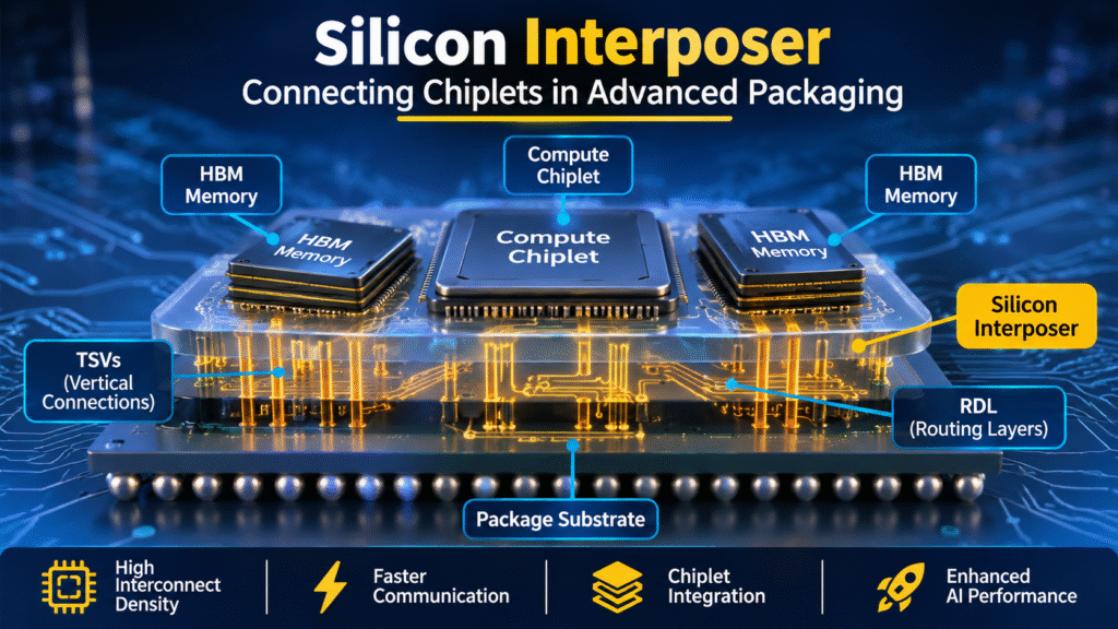
Silicon interposers enable high-density connections between chiplets, processors, and high-bandwidth memory (HBM). They play an important role in advanced semiconductor packaging, particularly in AI accelerators, GPUs, and high-performance computing systems.
In this article, we explore how silicon interposers work, their architecture, benefits, design challenges, and applications in modern electronics.
What Is a Silicon Interposer?
A silicon interposer is a thin silicon layer placed between semiconductor dies and the package substrate. It provides fine-pitch electrical connections between multiple chips.
Unlike a traditional package substrate, a silicon interposer can support much denser wiring. This allows chiplets and memory devices to communicate through short, high-density connections.
A typical silicon interposer contains:
- Through-Silicon Vias (TSVs): Vertical electrical connections through the silicon layer.
- Redistribution Layers (RDL): Metal routing layers that connect different dies.
- Microbumps: Small conductive connections between semiconductor dies and the interposer.
- Silicon Base: The structural layer that supports the routing network.
Together, these components create a compact connection platform for multiple semiconductor dies.
Why Are Silicon Interposers Important?
Traditional semiconductor designs often integrate most processing functions into a single large chip. However, manufacturing large chips can become expensive and technically challenging.
Chiplet-based designs offer another approach. Different functions can be manufactured as separate dies and then connected inside one package.
However, these chiplets need fast and reliable communication.
This is where silicon interposers become useful. They provide dense routing between dies while reducing the physical distance that signals need to travel.
As a result, advanced packaging can support:
- Higher interconnect density.
- Shorter communication paths between chiplets.
- Efficient connections to high-bandwidth memory.
- Flexible integration of different semiconductor technologies.
- Scalable processor and accelerator designs.
How Does a Silicon Interposer Work?
A silicon interposer acts as an electrical connection layer between multiple semiconductor dies.
Consider an AI accelerator package containing a compute chiplet and several HBM stacks.
The compute die performs processing operations, while HBM provides high-bandwidth memory access. Both are mounted on the silicon interposer.
The interposer contains fine-pitch metal routing that connects these components. Signals travel between the compute die and memory through these routing layers.
Additionally, TSVs provide vertical electrical paths between the interposer and the package substrate.
This arrangement supports high-density communication within a compact package.
Main Components of a Silicon Interposer
1. Through-Silicon Vias (TSVs)
TSVs are vertical conductive structures that pass through a silicon wafer or die.
They connect routing layers on different sides of the interposer. Copper is commonly used as the conductive material.
TSVs help transfer electrical signals and power between the upper chip connections and the package substrate.
2. Redistribution Layers (RDL)
Redistribution layers contain fine copper traces that route electrical signals across the interposer.
They connect different chiplet terminals and help organize signal paths.
Furthermore, careful RDL design is important for maintaining signal integrity and supporting high-speed communication.
3. Microbumps
Microbumps are small conductive connections used to attach semiconductor dies to the interposer.
Their small size allows designers to create a large number of connections within a limited area.
Consequently, microbumps are important for high-density chiplet integration.
4. Silicon Substrate
The silicon base provides mechanical support for the interposer routing structure.
It also provides a suitable platform for fine-pitch fabrication processes. However, its electrical and thermal properties must be considered during package design.
Silicon Interposers in 2.5D Packaging
Silicon interposers are widely used in 2.5D semiconductor packaging.
In this architecture, multiple dies are placed side by side on an interposer instead of stacking all the dies vertically.
For example, an AI processor can be placed next to several HBM stacks on the same silicon interposer.
The interposer provides high-density connections between these components. Meanwhile, TSVs connect the interposer to the package substrate.
This approach allows manufacturers to integrate different chiplets into one advanced package.
One well-known commercial example is TSMC’s CoWoS technology, which supports the integration of multiple system-on-chip dies and HBM stacks.
Silicon Interposer vs. Silicon Bridge
Silicon interposers and silicon bridges both support high-density communication between chiplets. However, their physical structures are different.
| Feature | Silicon Interposer | Silicon Bridge |
|---|---|---|
| Structure | Larger silicon layer | Small silicon connection section |
| Routing | Across a larger package area | Focused between selected dies |
| Integration | Multiple dies can share one interposer | Connects selected chiplet edges |
| Design complexity | Requires larger interposer fabrication | Requires localized bridge integration |
| Applications | AI accelerators and high-performance computing | Multi-die processor packages |
For example, TSMC CoWoS-S uses a full silicon interposer, while Intel’s EMIB technology uses embedded silicon bridges to connect dies.
The right approach depends on package size, routing requirements, manufacturing cost, and performance targets.
Benefits of Silicon Interposers
Silicon interposers offer several advantages in advanced semiconductor packaging.
1. High Interconnect Density
Fine-pitch routing supports a large number of connections between chiplets.
This is especially important for AI accelerators that need fast communication with memory devices.
2. Improved Signal Communication
Shorter connections can reduce parasitic resistance, capacitance, and inductance compared with longer package-level routes.
As a result, designers can build high-speed connections between semiconductor dies.
3. HBM Integration
AI processors often require high memory bandwidth.
Silicon interposers allow compute dies and HBM stacks to be placed close together, supporting wide memory interfaces.
4. Chiplet Integration
Different chiplets can be manufactured using different semiconductor process technologies.
After fabrication, these dies can be integrated into a single package through the interposer.
Therefore, manufacturers have more flexibility when designing complex semiconductor systems.
5. Compact Package Design
By placing multiple dies on a shared interconnection platform, designers can integrate several functions into one package.
This is useful for systems that require high performance within limited physical space.
Challenges in Silicon Interposer Design
Although silicon interposers provide several advantages, their design and manufacturing involve important challenges.
1. Manufacturing Cost
Silicon interposers require advanced fabrication processes and fine-pitch routing.
Larger interposers also require more silicon area, which can increase manufacturing costs.
2. Thermal Management
AI processors and HBM stacks generate significant heat during operation.
Because multiple dies are placed close together, thermal interaction between components becomes an important design consideration.
Therefore, engineers must evaluate heat distribution, cooling solutions, and temperature limits.
3. Signal Integrity
High-speed signals travel through dense routing structures.
Poor routing, impedance discontinuities, and crosstalk can affect signal quality.
For this reason, package designers must perform signal integrity analysis before manufacturing.
4. Mechanical Reliability
Differences in thermal expansion between silicon, copper, and package materials can create mechanical stress.
These stresses may affect microbumps, TSV structures, and package connections.
Consequently, thermal cycling and mechanical reliability testing are important.
5. Manufacturing Yield
As package complexity increases, defects in individual dies or interposer connections can affect the final product.
Manufacturers must carefully control fabrication, bonding, inspection, and assembly processes.
Applications of Silicon Interposers
Silicon interposers are useful in several advanced computing applications.
AI accelerators: They connect compute dies with HBM stacks to support demanding AI workloads.
Graphics Processing Units: Advanced GPU packages can use interposers to connect multiple dies and memory components.
High-Performance Computing: HPC systems require high-speed communication between processing and memory components.
Networking hardware: High-performance networking devices can benefit from dense connections between processing and communication chips.
Advanced processors: Chiplet-based processor designs use advanced packaging to integrate different functional dies.
Silicon Interposers and the Future of AI Hardware
AI hardware is moving toward more complex semiconductor packages. Instead of depending entirely on one large chip, manufacturers are increasingly exploring chiplet-based architectures and advanced packaging technologies.
Silicon interposers provide an important connection platform for these designs.
However, future improvements will also depend on better thermal management, more reliable bonding techniques, improved manufacturing yields, and alternative interposer materials.
Technologies such as glass interposers, silicon bridges, and hybrid bonding are also being developed to address different packaging requirements.
As semiconductor integration advances, interposer technology will remain an important part of high-performance computing and AI hardware.
Frequently Asked Questions (FAQs)
1. What is a silicon interposer?
A silicon interposer is a thin silicon layer that provides high-density electrical connections between multiple semiconductor dies inside an advanced package.
2. What is the main purpose of a silicon interposer?
Its main purpose is to connect chiplets and memory devices using dense routing and short electrical paths.
3. What are TSVs in silicon interposers?
Through-Silicon Vias are vertical conductive connections that pass through the silicon layer and connect different routing levels.
4. What is the difference between 2.5D and 3D packaging?
In 2.5D packaging, multiple dies are generally placed side by side on an interposer. In 3D packaging, dies are stacked vertically to create a more compact integration structure.
5. Why are silicon interposers important for AI chips?
They enable dense connections between AI processors and HBM stacks, supporting the high-bandwidth communication required by demanding AI workloads.
6. Are silicon interposers expensive?
They can be expensive because they require advanced fabrication, fine-pitch routing, and complex assembly processes. Actual cost depends on package size, design, and manufacturing yield.
Conclusion
Silicon interposers are an important technology in modern semiconductor packaging. They enable high-density connections between chiplets, processors, and memory devices while supporting advanced 2.5D integration.
As AI accelerators and high-performance processors become more complex, silicon interposers will continue to support the development of powerful and scalable semiconductor systems.
Whether you’re exploring new ideas, learning something new, or looking for opportunities, Enigma Community brings you closer to a world of possibilities.
Join Us: https://www.enigmacommunity.com/