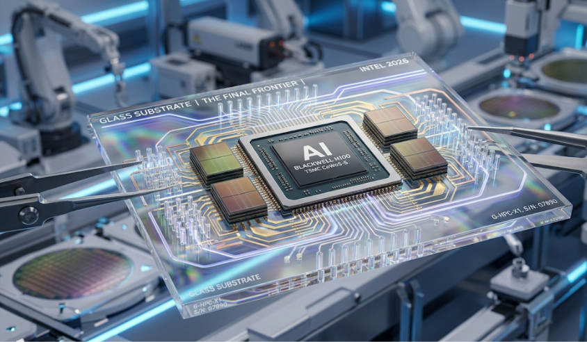
The shift toward Glass Substrates represents the most significant breakthrough in semiconductor packaging since the 1970s. As the world transitions into the era of trillion-transistor AI chips, our traditional foundations—organic plastic resins—are physically failing to support the weight of modern computing.
The “Silicon Ceiling”
For decades, we have used Organic Substrates (specifically Ajinomoto Build-up Film, or ABF) as the “flooring” that connects a silicon chip to a motherboard. However, as chips become larger and run hotter to handle AI workloads, these plastic layers began to warp and bend. This “warpage” causes microscopic connections to snap, creating a massive roadblock for companies like NVIDIA and Intel.
1. The Industrial Bottleneck: Why Organic Substrates are Failing
For over 20 years, the industry has relied on Organic (ABF) Substrates. While cost-effective, they are hitting physical limits in the AI era:
- Thermal Instability: High-performance AI chips generate intense heat, causing organic materials to warp and expand. This “warpage” breaks the microscopic solder connections.
- Size Constraints: As chips grow larger (multi-die packages), plastic becomes too flexible to maintain the perfect flatness required for lithography.
- Interconnect Density: We have reached the minimum distance possible for drilling holes in plastic without structural failure.
2. The Engineering Advantage of Glass
Glass is being adopted not just as a “board,” but as a high-performance component.
- Extreme Flatness: Glass is 3–5 times flatter than organic materials. This allows for tighter “Depth of Focus” during manufacturing, meaning more circuits in less space.
- Matched CTE (Coefficient of Thermal Expansion): The expansion rate of glass is much closer to silicon than plastic is. This reduces mechanical stress and prevents “chip-snap” during heating cycles.
- TGV Technology: Through-Glass Vias (TGVs) are vertical tunnels drilled by lasers. Because glass is rigid, these vias can be placed 10x closer together than holes in plastic, enabling massive data throughput.
3. The Optical Revolution: Silicon Photonics
The most significant long-term benefit of glass is its transparency.
- Light over Electricity: As copper wires hit a “speed limit,” glass substrates allow for the integration of Optical Waveguides.
- Integrated Photonics: Data can be sent via light pulses directly through the substrate. This transition reduces power consumption by roughly 40% and eliminates the heat generated by traditional electrical resistance.
4. Comparative Analysis: Glass vs. Organic
| Specification | Organic (ABF) | Glass Substrate |
| Operating Temp | Up to 150°C | 250°C – 600°C+ |
| Surface Flatness | Low (Warp-prone) | High (Ultra-stable) |
| Vias (Vertical Holes) | Mechanical/Laser Drill | Precision Laser-Induced |
| Data Signaling | Electrical (Copper) | Hybrid (Electrical + Optical) |
| Recyclability | Difficult/Toxic Resins | High (Inert & Reusable) |
5. Security and the “Hardware Fingerprint”
Glass introduces a new layer of cybersecurity: Optical PUFs (Physically Unclonable Functions).
Because every piece of glass has unique, microscopic internal structures, a laser shone through the substrate creates a “speckle pattern.” This pattern is impossible to replicate, providing a physical, un-hackable identity for every chip manufactured.
6. Market Outlook (2026 and Beyond)
- Intel: Leading with high-volume manufacturing lines in Arizona.
- Samsung: Utilizing glass for the next generation of HBM4 (High Bandwidth Memory).
- Apple: Investigating glass for ultra-thin, power-efficient mobile processors.
Conclusion
The transition to glass represents the end of “disposable” hardware architecture. We are entering an era where the substrate is as intelligent and capable as the silicon it holds. Glass is the only material capable of sustaining the exponential growth of AI, 6G, and quantum computing.