
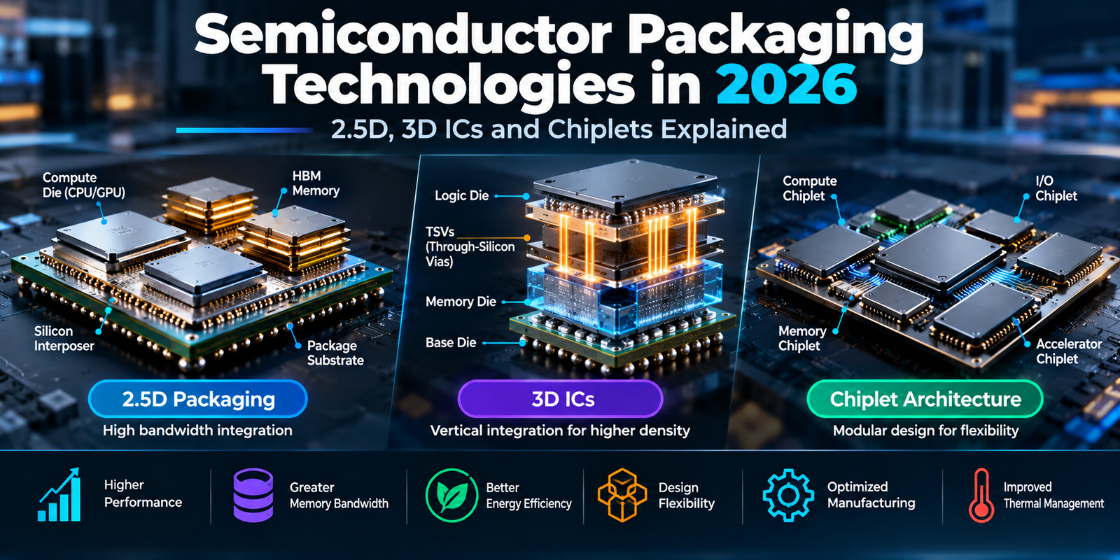
Semiconductor Packaging Technologies in 2026: 2.5D, 3D ICs and Chiplets Explained
SEO Title: Semiconductor Packaging Technologies in 2026: 2.5D, 3D ICs & Chiplets
Focus Keyphrase: Semiconductor Packaging Technologies
URL Slug: semiconductor-packaging-technologies-2026
Meta Description: Explore semiconductor packaging technologies in 2026, including 2.5D packaging, 3D ICs, chiplets, advanced interconnects, and AI hardware.
Excerpt: Advanced semiconductor packaging is transforming chip design. Learn how 2.5D packaging, 3D integrated circuits, and chiplet architectures improve performance, memory bandwidth, and integration.
Introduction
Semiconductor technology continues to evolve as artificial intelligence, high-performance computing, automotive electronics, and connected devices demand faster and more efficient hardware. Traditionally, semiconductor manufacturers focused on shrinking transistors and increasing the number of components integrated onto a single silicon die. However, continued scaling presents significant challenges related to manufacturing costs, power consumption, heat generation, and design complexity.
This is where semiconductor packaging technologies are becoming increasingly important.
Advanced packaging allows manufacturers to integrate multiple silicon dies, memory components, and specialized processing units into a single package. Instead of relying entirely on one large chip, engineers can combine smaller components to create powerful and flexible computing systems.
Technologies such as 2.5D packaging, 3D integrated circuits (3D ICs), and chiplet architectures are helping address the growing demands of modern processors.
These approaches are particularly relevant to AI accelerators, graphics processing units (GPUs), high-performance CPUs, and data center hardware.
Understanding these technologies helps hardware engineers make informed decisions about processor architecture, thermal management, power delivery, and system integration.
In this article, we explore how advanced semiconductor packaging works, explain the differences between 2.5D and 3D integration, and examine the advantages and challenges of chiplet-based designs.
1. What Is Semiconductor Packaging?
Semiconductor packaging is the process of enclosing and connecting a semiconductor die so it can operate reliably within an electronic system.
A silicon die contains the transistors and electronic circuits that perform computing, memory, or other functions. However, the die needs electrical connections, physical protection, and a suitable way to transfer heat before it can be used in a product.
Traditional semiconductor packages connect a single die to a substrate, which provides electrical connections to the circuit board.
Advanced packaging goes further by integrating multiple dies or components into one package.
These components may include:
- CPU and GPU dies.
- High-bandwidth memory (HBM).
- Input/output controllers.
- Specialized AI accelerators.
- Cache memory.
- Communication and networking components.
Instead of manufacturing every function on one large die, engineers can integrate components that use different manufacturing processes.
For example, a high-performance AI processor may combine computing dies manufactured using an advanced process with input/output dies manufactured using a more cost-effective process.
This approach allows engineers to optimize different parts of the system independently.
Why Is Advanced Packaging Important?
Advanced packaging addresses several challenges associated with modern semiconductor design.
Improved integration: Multiple dies can operate together within a compact package.
Higher bandwidth: Shorter, denser connections can improve communication between processors and memory.
Design flexibility: Different components can be developed and manufactured using suitable technologies.
Potential manufacturing advantages: Smaller dies can improve manufacturing yield in some designs, although packaging and integration costs must also be considered.
Specialized computing: Designers can combine CPUs, GPUs, memory, and accelerators according to application requirements.
As processors become more complex, packaging is increasingly important to overall system performance.
2. What Is 2.5D Semiconductor Packaging?
2.5D packaging is an advanced integration technique in which multiple silicon dies are placed side by side and connected through a high-density interconnect structure.
This structure may use a silicon interposer, an organic interposer, or another suitable packaging technology.
The term 2.5D distinguishes this approach from conventional side-by-side packaging and fully vertical 3D die stacking.
Although the dies are not necessarily stacked directly on top of each other, they can communicate through dense connections within the package.
How Does 2.5D Packaging Work?
A typical 2.5D package may contain the following components:
- Computing dies: These perform processing and acceleration tasks.
- Memory dies: These supply data to the computing components.
- Interposer or interconnect structure: This provides dense electrical connections between the dies.
- Package substrate: This connects the integrated components to the circuit board.
- Thermal management components: These help remove heat generated during operation.
For example, an AI accelerator may place several computing dies alongside HBM stacks.
The interconnect structure allows the accelerator to communicate with memory through a wide interface, supporting high data-transfer rates.
This is valuable for AI workloads that repeatedly move large amounts of data between memory and processing units.
Advantages of 2.5D Packaging
1. High memory bandwidth
Dense connections between computing dies and HBM can support high memory bandwidth.
2. Better integration
Multiple components can be combined within one package without requiring all functions to be implemented on a single die.
3. Flexible manufacturing
Different dies may use different semiconductor processes, depending on the package design.
4. Potentially improved performance
Shorter communication paths and high-density interconnects can reduce certain data-transfer bottlenecks.
Challenges of 2.5D Packaging
Despite its advantages, 2.5D packaging presents several engineering challenges.
- Interposer and substrate design can be complex.
- High-density connections require careful signal-integrity analysis.
- Power delivery must support demanding computing loads.
- Thermal management becomes more complicated as package power increases.
- Packaging costs can be substantial.
- Manufacturing, assembly, and testing require specialized processes.
Therefore, 2.5D packaging is particularly useful when a design needs high-bandwidth communication between multiple dies, but its suitability depends on performance requirements and manufacturing economics.
3. What Are 3D Integrated Circuits (3D ICs)?
Three-dimensional integrated circuits, commonly called 3D ICs, integrate multiple semiconductor dies or active device layers vertically.
Instead of placing all components side by side, engineers stack them to create a more compact structure.
Vertical integration can reduce the distance that signals travel between certain components and increase integration density.
Depending on the design, the stacked components may communicate through through-silicon vias (TSVs), hybrid bonding, or other vertical interconnect technologies.
How Does 3D IC Technology Work?
A 3D IC package may contain multiple dies stacked vertically.
Each die can perform a particular function, such as processing, memory storage, or cache operations.
Vertical interconnects provide communication between the layers.
For example, stacked memory devices can use vertical connections to communicate between memory dies. In other designs, hybrid bonding can create very dense connections between vertically integrated components.
The exact architecture depends on the intended application and manufacturing process.
Advantages of 3D ICs
Higher integration density: Vertical stacking can accommodate more functionality within a smaller footprint.
Shorter communication paths: Signals can travel shorter distances between vertically connected components.
Potential bandwidth improvements: Dense vertical connections can support communication between stacked dies.
Flexible system design: Different layers can perform different functions.
Reduced footprint: Vertical integration can reduce the area occupied by some components compared with equivalent side-by-side arrangements.
Challenges of 3D ICs
The main challenge is managing the additional complexity introduced by vertical integration.
Heat generated by internal layers may be difficult to remove, especially when multiple high-power computing dies are stacked.
Engineers must also consider:
- Thermal resistance between layers.
- Power delivery to each die.
- Vertical interconnect reliability.
- Manufacturing yield.
- Testing and fault isolation.
- Mechanical stress and package reliability.
- Cost and process complexity.
Consequently, 3D integration requires close coordination between circuit design, packaging, thermal engineering, and manufacturing.
4. What Are Chiplets?
Chiplets are smaller semiconductor dies designed to work together as components of a larger processor or integrated system.
Rather than implementing every function on one large die, engineers divide the design into multiple dies.
Each chiplet may perform a specific task, such as general-purpose computing, graphics processing, input/output operations, or memory control.
These chiplets are integrated within a package and communicate through suitable interconnects.
Chiplet-based architectures are increasingly important because they provide an alternative to designing very large monolithic processors.
How Do Chiplet Architectures Work?
A chiplet-based processor typically includes several functional components.
For example, a processor may combine:
- CPU compute chiplets.
- Input/output chiplets.
- Memory controllers.
- Cache components.
- Specialized acceleration dies.
The package connects these components so they can operate as a coordinated system.
The interconnect must provide sufficient bandwidth and acceptable latency for the intended workload.
Some designs use proprietary interconnects, while others can use standards such as Universal Chiplet Interconnect Express (UCIe), where supported.
The availability of compatible interfaces and packaging technologies influences how easily chiplets from different sources can be integrated.
Advantages of Chiplet Design
1. Modular architecture
Engineers can divide a complex processor into smaller functional blocks.
2. Manufacturing flexibility
Different chiplets may be manufactured using different process technologies.
3. Potential yield advantages
Smaller individual dies may be easier to manufacture successfully than one very large die. However, overall package yield also depends on the number of dies, assembly quality, and testing.
4. Design reuse
A compatible chiplet may be reused across multiple products, reducing the need to redesign every component.
5. Product scalability
Manufacturers can develop different configurations by changing the number or type of chiplets.
Challenges of Chiplet Architectures
Chiplets also introduce several important design considerations.
- Communication between chiplets can add latency and consume power.
- Interconnect protocols must be compatible.
- Package design becomes more complex.
- Thermal management must account for multiple heat-generating components.
- Testing must identify faults across the integrated system.
- Integration and assembly costs may offset some manufacturing savings.
Chiplets are therefore not automatically cheaper or faster than monolithic designs. Their value depends on how effectively the complete system is engineered.
5. 2.5D vs 3D ICs vs Chiplets: Key Differences
Although these technologies are related, they describe different aspects of semiconductor integration.
2.5D and 3D describe packaging or integration arrangements, while chiplet describes a modular die-based design approach.
A chiplet-based processor may use 2.5D packaging, 3D integration, or a combination of both.
The following table summarizes their main differences.
| Feature | 2.5D Packaging | 3D IC Integration | Chiplet Architecture |
|---|---|---|---|
| Basic approach | Multiple dies placed side by side with dense interconnects | Dies or active layers integrated vertically | System divided into multiple functional dies |
| Physical arrangement | Primarily side by side | Vertically stacked | Side by side, stacked, or both |
| Common interconnects | Interposers and high-density package routing | TSVs, hybrid bonding, or other vertical connections | Package-level or die-to-die interconnects |
| Main advantage | High-bandwidth communication between dies | High integration density and short vertical connections | Modular and flexible system design |
| Major challenge | Interposer cost, signal integrity, and power delivery | Thermal management and vertical integration complexity | Interoperability, testing, and system integration |
| Typical applications | AI accelerators and high-performance computing | Stacked memory and selected processor designs | CPUs, GPUs, AI accelerators, and specialized systems |
The correct technology depends on the system’s performance requirements, physical constraints, manufacturing options, and cost targets.
6. How Advanced Packaging Improves AI Processor Performance
Artificial intelligence workloads place substantial demands on computing hardware.
AI processors must execute mathematical operations while continuously moving model parameters, input data, and intermediate results between memory and processing units.
When these data transfers become a bottleneck, increasing the number of computing units may not significantly improve overall performance.
Advanced packaging helps address this problem by improving how different components communicate.
High-Bandwidth Memory Integration
AI accelerators often require high memory bandwidth to keep their computing units supplied with data.
Packaging techniques that integrate HBM close to processing dies can support wide, high-speed memory connections.
This can improve data availability for memory-intensive workloads.
Reduced Interconnect Distance
Communication between separate chips on a circuit board may involve longer electrical paths than communication through dense package-level interconnects.
Advanced packaging can shorten certain connections and provide more interconnect density.
Depending on the implementation, this can reduce communication overhead and improve system efficiency.
Specialized Processing Components
Chiplet architectures allow different computing functions to be implemented in separate dies.
For example, a system can combine general-purpose processor cores with dedicated accelerators.
This approach allows engineers to select suitable computing components for different workloads.
Better Integration of Computing and Memory
Some workloads benefit from placing memory and processing components close together.
Advanced packaging can support such arrangements, although the actual performance benefit depends on memory architecture, data-access patterns, and software behavior.
The key takeaway: Advanced packaging improves AI hardware by optimizing communication and integration, not simply by increasing the number of transistors.
7. Thermal Management Challenges in Advanced Packaging
Thermal management is one of the most important considerations in advanced semiconductor packaging.
Modern processors can generate substantial heat within a small physical area.
When multiple dies are integrated into a single package, heat from different components can interact and create complex temperature distributions.
This becomes particularly challenging in 3D ICs, where some layers may have limited direct access to a heat spreader.
Why Does Heat Affect Performance?
Excessive temperature can cause a processor to reduce its operating frequency or power consumption to remain within safe operating limits.
This behavior, known as thermal throttling, can reduce performance.
Persistent thermal stress can also affect reliability and packaging materials.
Thermal Challenges in 2.5D Packaging
In 2.5D designs, multiple high-performance dies may be positioned close together.
Their combined power consumption can create concentrated heat loads.
Engineers must consider die placement, heat spreaders, thermal interface materials, package substrates, and cooling solutions.
Thermal Challenges in 3D ICs
In vertically stacked designs, heat generated by internal layers may need to pass through other layers before reaching the cooling system.
This can increase thermal resistance.
Engineers may need to optimize the placement of high-power components, improve thermal paths, and carefully manage power distribution.
How Can Engineers Improve Thermal Performance?
Several strategies can help manage heat:
- Optimize the placement of heat-generating components.
- Select appropriate thermal interface materials.
- Improve heat-spreader and heat-sink designs.
- Evaluate liquid cooling for demanding systems where appropriate.
- Model temperature distributions before manufacturing.
- Balance workload placement and power consumption.
- Test the complete package under realistic operating conditions.
Thermal simulation and physical testing are especially important because package-level thermal behavior can differ significantly from the behavior of an individual die.
8. The Role of PCB Design in Advanced Semiconductor Packaging
Advanced semiconductor packaging does not operate independently of the printed circuit board.
The package must connect to the PCB through a suitable interface while maintaining electrical performance, mechanical reliability, and thermal stability.
As data rates increase, PCB design becomes more demanding.
Signal Integrity
High-speed signals can be affected by impedance mismatches, reflections, crosstalk, and electromagnetic interference.
Engineers must design PCB routing and package connections to maintain signal quality.
This may involve controlled-impedance traces, appropriate reference planes, careful connector selection, and high-speed simulation.
Power Integrity
AI processors and high-performance computing devices may require substantial current and stable supply voltages.
The PCB and package power delivery network must minimize voltage fluctuations and power distribution losses.
Engineers may use carefully designed power planes, decoupling capacitors, and power-integrity simulations to address these challenges.
Thermal Design
The PCB contributes to the overall thermal behavior of the system.
Copper distribution, thermal vias, component placement, heat spreaders, and airflow can all affect heat removal.
In some designs, the PCB also serves as a mechanical platform that must tolerate thermal expansion and assembly stresses.
Manufacturing and Reliability
Fine-pitch package connections require appropriate PCB fabrication and assembly capabilities.
Engineers must consider pad geometry, soldering processes, board warpage, inspection methods, and reliability testing.
A well-designed semiconductor package still requires a compatible PCB to achieve its intended performance.
9. Applications of Advanced Semiconductor Packaging
Advanced packaging is used in several areas of modern electronics.
Artificial Intelligence and Data Centers
AI accelerators can combine computing dies with high-bandwidth memory to support demanding training and inference workloads.
High-density integration helps address bandwidth and packaging constraints.
High-Performance CPUs and GPUs
Chiplet architectures can allow processor manufacturers to combine computing, memory-control, and input/output functions within one package.
This can support different product configurations and manufacturing strategies.
Automotive Electronics
Advanced packaging can support computing, sensing, and communication components used in automotive systems.
However, automotive applications also require appropriate qualification, reliability validation, and safety-related engineering processes.
Networking and Telecommunications
High-speed networking equipment depends on processors, switching components, and communication devices that require efficient electrical connections and thermal management.
Advanced packaging can support the integration of these components.
Mobile and Consumer Electronics
Compact devices benefit from packaging techniques that reduce physical size while integrating processors, memory, and other components.
The appropriate approach depends on cost, power consumption, manufacturing requirements, and product constraints.
10. Manufacturing Challenges and Cost Considerations
Advanced packaging can improve integration and performance, but it introduces manufacturing and economic challenges.
These challenges become more significant as designs combine more dies, finer interconnects, and increasingly complex package structures.
Manufacturing Yield
Each die must meet the required specifications, and the assembled package must function correctly.
When several dies are combined, defects in individual components or assembly processes can affect the final product.
Known-good-die testing, package inspection, and system-level validation help reduce these risks.
Packaging Equipment
Advanced integration may require specialized bonding, interconnect, inspection, and testing equipment.
The availability and capacity of these manufacturing processes can influence production schedules and costs.
Design Complexity
Engineers must coordinate semiconductor design, package layout, PCB integration, thermal analysis, and electrical verification.
This requires collaboration across multiple engineering disciplines.
Testing Requirements
Testing becomes more complex when several dies communicate within a package.
Engineers need appropriate methods to identify faults, validate die-to-die communication, and confirm operation under expected conditions.
Total Cost of Ownership
The cheapest packaging approach is not necessarily the most economical solution overall.
Businesses should evaluate development costs, manufacturing yield, assembly expenses, testing requirements, thermal management, and product performance.
For high-volume products, even small improvements in yield or assembly efficiency can significantly affect overall costs.
11. How to Choose the Right Semiconductor Packaging Technology
Selecting a packaging technology requires a clear understanding of the intended application.
A high-performance AI accelerator may require high-bandwidth memory and dense die-to-die connections. A cost-sensitive embedded device may not need the complexity of advanced multi-die integration.
Engineers should evaluate the following factors before selecting a packaging approach.
| Evaluation Factor | Questions to Consider |
|---|---|
| Performance | What computing throughput and communication bandwidth are required? |
| Memory | Does the application require HBM or other high-bandwidth memory? |
| Power consumption | What are the package’s power delivery requirements? |
| Thermal management | How will heat be removed from each die? |
| Physical size | Are there strict package dimensions or height limits? |
| Manufacturing | Are suitable fabrication and assembly capabilities available? |
| Reliability | What environmental and operating conditions must the package tolerate? |
| Testing | How will individual dies and the assembled package be validated? |
| Cost | What are the development, manufacturing, assembly, and testing costs? |
| Scalability | Can the design accommodate future product requirements? |
When Should Engineers Consider 2.5D Packaging?
Consider 2.5D packaging when multiple dies need dense, high-bandwidth communication and the design benefits from placing components side by side.
When Should Engineers Consider 3D Integration?
Consider 3D integration when vertical stacking provides meaningful benefits in integration density, communication distance, or memory organization, and the thermal and manufacturing requirements can be managed.
When Should Engineers Consider Chiplets?
Consider a chiplet architecture when modular design, component reuse, process flexibility, or product scalability provides a meaningful advantage.
These approaches are not mutually exclusive. A chiplet-based design can use both 2.5D and 3D integration.
The best solution is the one that satisfies the system requirements while balancing performance, cost, reliability, and manufacturability.
Conclusion
Semiconductor packaging has become a critical part of modern hardware engineering.
As AI, high-performance computing, automotive electronics, and connected devices demand more capable processors, advanced packaging technologies provide new ways to integrate computing, memory, and communication components.
2.5D packaging supports dense connections between side-by-side dies, while 3D ICs enable vertical integration. Chiplet architectures divide complex processors into modular components that can be combined within a single package.
Each approach offers distinct advantages, but all require careful consideration of thermal management, signal integrity, power delivery, manufacturing yield, and testing.
For hardware engineers, understanding these technologies is essential when designing high-performance and reliable electronic systems.
As semiconductor development continues to evolve, advanced packaging will remain an important part of building efficient processors and specialized computing hardware.
At Hashing Hardware, exploring semiconductor packaging technologies helps engineers understand the design decisions shaping the next generation of computing systems.