
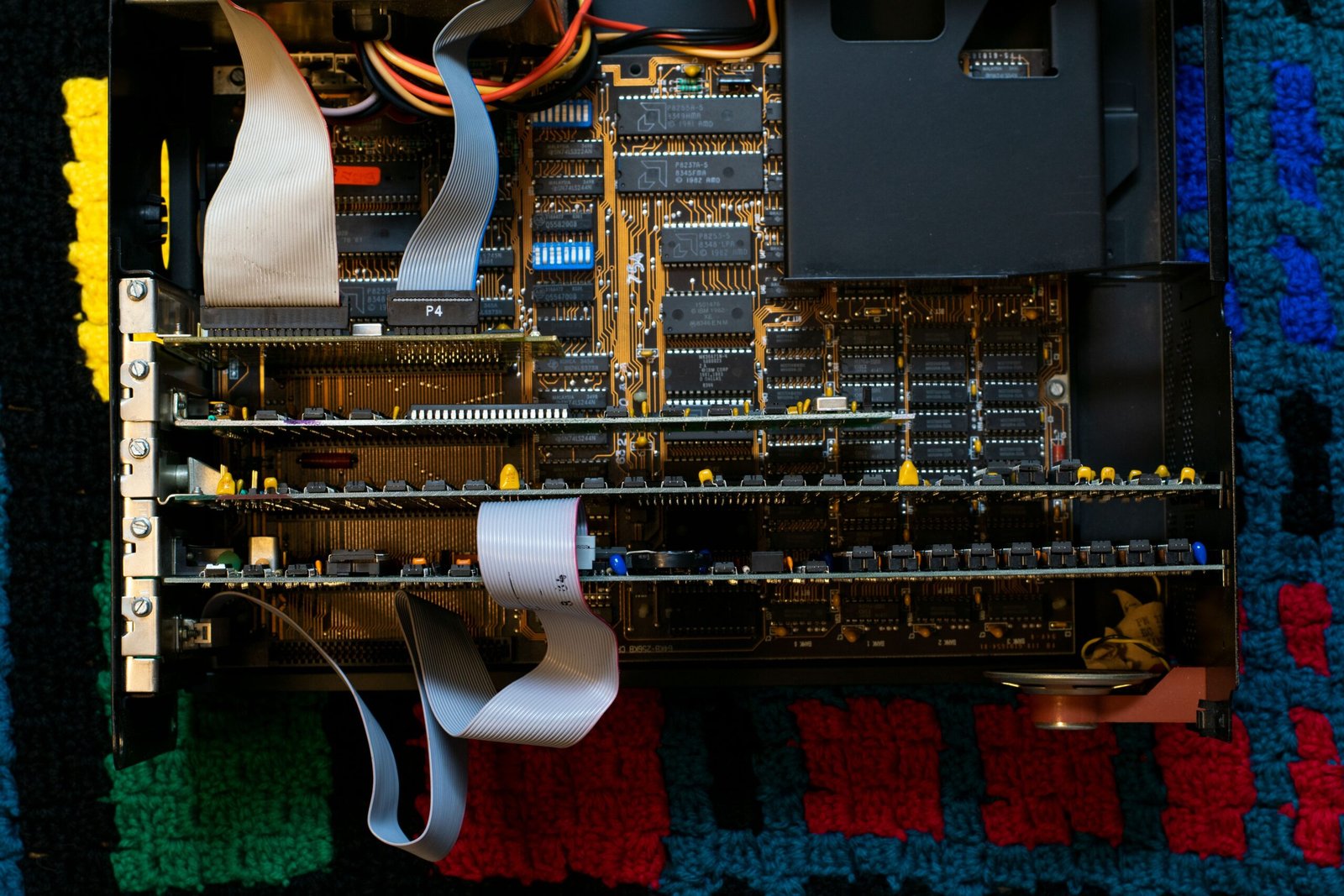
Universal chip interconnects have quietly solved one of the chip industry’s oldest problems. Chiplets from different companies could not talk to each other. Every vendor built its own proprietary connection. Universal chip interconnects changed that entirely. One open standard now lets chiplets from Intel, AMD, TSMC, and dozens of other companies work together in the same package. Here is how this happened, and why it matters so much right now.
What Universal Chip Interconnects Actually Solve
Chiplets brought real benefits to chip design. Smaller pieces mean better yield and lower cost. But early chiplet designs had a serious catch. Each company built its own private connection method. A chiplet from one vendor simply could not talk to a chiplet from another.
Universal Chiplet Interconnect Express, or UCIe, fixed that problem directly. It works like PCIe, but at the microscopic scale between individual dies instead of between full boards. Therefore, universal chip interconnects let chiplets manufactured by different foundries, on different process nodes, work together inside one shared package.
Why 2026 Marks a Real Turning Point
Universal chip interconnects have crossed from promising idea into mainstream infrastructure this year. The UCIe Consortium has grown past 120 members. That list includes Intel, AMD, TSMC, Samsung, ARM, Meta, and Google. Consequently, proprietary die-to-die links now look increasingly outdated outside single-vendor ecosystems.
Three forces pushed this shift forward at once. Moore’s Law slowed down badly below 3nm, making chiplets the more practical path to further gains. AI compute demand exploded too, with modern models needing 10 to 100 times the memory bandwidth of 2020 systems. Meanwhile, UCIe itself simply reached critical mass. Once enough major players adopt one standard, holding out with a private alternative stops making sense.
The Numbers Behind Universal Chip Interconnects
Raw performance numbers explain why UCIe caught on so fast. The UCIe 1.1 standard delivers roughly ten times better energy efficiency than PCIe Gen 5, the interconnect standard still common across most data centers. That efficiency gain matters enormously at scale.
Bandwidth density tells an even bigger story. UCIe’s linear bandwidth reaches 28 to 224 gigabytes per second per millimeter in a standard package. Advanced packaging configurations push that range up to 165 to 1,317 gigabytes per second per millimeter. That represents somewhere between 20 and over 100 times better performance than PCIe delivers today. UCIe 2.0, expected in 2026 to 2027, pushes further still, targeting 64 Gbps data rates alongside new optical die-to-die options.
How Universal Chip Interconnects Power Modular Computing
The real promise behind universal chip interconnects is modularity. Instead of designing one massive chip from scratch, engineers can now mix specialized pieces built by different companies. A compute chiplet from one vendor. A memory controller from another. All connected through the same shared standard.
This flexibility matters most in AI hardware right now. UCIe enables high-speed communication between specialized processing units inside AI accelerators, improving overall computational efficiency across the whole system. High-performance computing benefits too, since chiplets can communicate with low latency and high bandwidth regardless of which company originally designed each piece.
Advanced Packaging Makes It All Physical
Universal chip interconnects only work because advanced packaging technology caught up too. TSMC’s CoWoS platform leads this space, supporting up to eight HBM4 memory stacks alongside compute chiplets in its newest generation. Intel’s competing EMIB approach embeds a small silicon bridge inside an organic substrate instead of using a full silicon interposer.
Hybrid bonding pushes density even further. TSMC’s SoIC and Intel’s Foveros Direct now achieve sub-10 micron bonding pitches, packing far more connections into the same physical space than older micro-bump methods allowed. Glass substrates are emerging too, offering lower signal loss and higher wiring density than the organic materials most packages still use today.
The Real Bottlenecks Still Standing
Universal chip interconnects have not solved every problem in the chiplet ecosystem. Advanced packaging capacity remains tightly constrained. TSMC’s CoWoS lead times currently run six to nine months, with Apple, NVIDIA, and AMD all competing for the same limited allocation slots.
Memory supply creates a second bottleneck. SK Hynix controls roughly 62% of the HBM market, with its entire 2026 production volume sold out well before the year even began. That concentration gives a small handful of memory suppliers enormous influence over which AI accelerator programs actually ship on schedule.
Geography adds a third layer of risk. Nearly all leading-edge CoWoS packaging capacity sits in Taiwan today. Any serious disruption there would immediately affect the vast majority of advanced packaging output worldwide, and neither Intel nor Samsung could absorb that demand quickly if it happened.
Where This Connects to Chip Manufacturing Itself
Universal chip interconnects and packaging innovation exist partly because traditional lithography scaling has gotten so much harder. When shrinking transistors stops delivering easy gains, connecting specialized chiplets together becomes the next practical lever. That same pressure is driving manufacturers to explore alternative paths at the lithography level too. For a closer look at how the industry is working around the limits of traditional chipmaking tools, read our full guide to chip manufacturing without EUV and the alternative paths emerging there.
Final Thought
Universal chip interconnects have turned chiplet-based design from a clever workaround into the industry’s default approach. UCIe’s rise past 120 consortium members, combined with real advanced packaging platforms like CoWoS and EMIB, has made mixing chiplets from different vendors a practical reality rather than a research goal. Real bottlenecks remain around packaging capacity, memory supply, and geographic concentration, and none of those get solved overnight. Still, the direction is clear. Modular, interoperable chip design is no longer the exception. It is quickly becoming how serious computing hardware gets built.