
Introduction
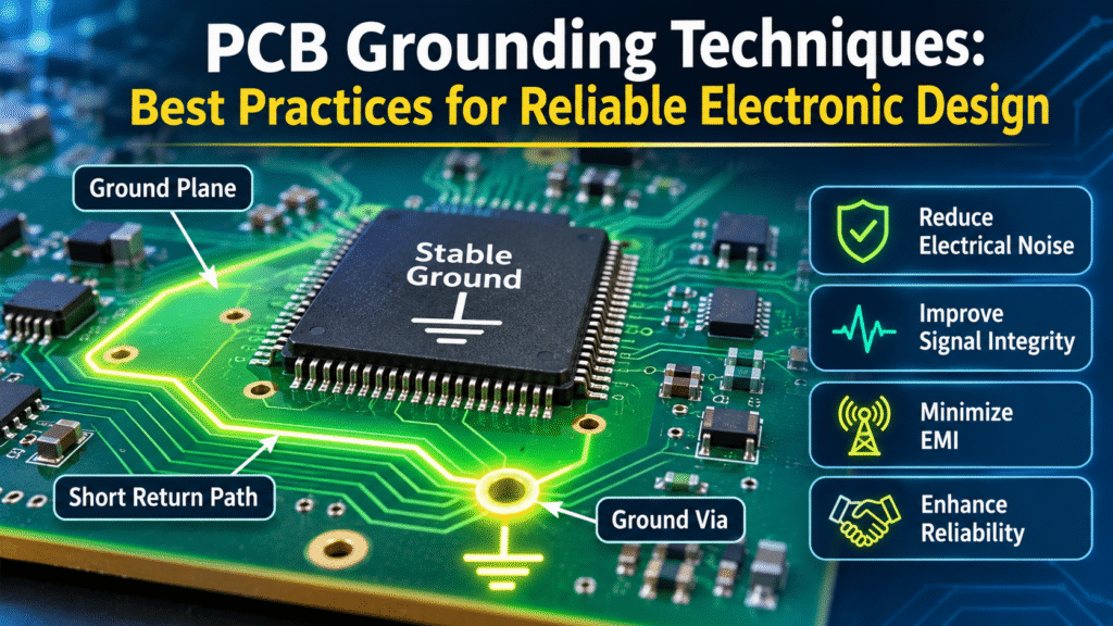
Grounding is one of the most important aspects of printed circuit board (PCB) design. A properly designed grounding system helps maintain signal quality, reduce electrical noise, minimize electromagnetic interference, and improve overall circuit reliability.
Modern electronic devices contain a combination of digital, analog, high-speed, and power circuits. Since these components generate different types of electrical currents, proper grounding is essential for stable operation.
However, poor grounding can lead to signal distortion, ground loops, unwanted noise, and unexpected circuit failures.
In this article, we explore different PCB grounding techniques, common design challenges, and practical guidelines that engineers can follow to develop reliable electronic hardware.
What Is Grounding in PCB Design?
Grounding in PCB design refers to creating a common electrical reference and providing a return path for current within an electronic circuit.
Every electrical circuit requires a complete current path. In other words, current flows from a power source through the circuit and returns to its source through an appropriate return path.
A PCB grounding system provides this return path while maintaining stable voltage references for connected components. As a result, it plays an important role in the overall performance of electronic devices.
Grounding is particularly important in:
- Digital electronic circuits
- Analog signal processing systems
- High-speed communication devices
- Power electronics
- RF and wireless systems
- Embedded hardware
Why Is PCB Grounding Important?
Proper grounding directly affects the performance and reliability of electronic circuits. Additionally, it helps prevent electrical problems that may affect the entire system.
1. Reduces Electrical Noise
Electronic components generate switching noise and unwanted electrical signals during operation.
A well-designed grounding system helps control these unwanted signals. Consequently, it reduces noise coupling between different circuit sections.
2. Improves Signal Integrity
High-speed signals require proper return-current paths to maintain signal quality.
For example, a continuous ground reference helps maintain consistent impedance. It also reduces signal reflections and distortion, improving overall signal integrity.
3. Minimizes Electromagnetic Interference
Poor grounding can create large current loops that increase electromagnetic radiation.
Therefore, proper grounding techniques help minimize loop areas and reduce unwanted electromagnetic emissions.
4. Prevents Ground Potential Differences
Different sections of a circuit may experience voltage differences because of current flowing through shared ground impedance.
A suitable grounding architecture helps minimize these differences. As a result, sensitive components can operate more reliably.
5. Improves Circuit Reliability
Stable grounding helps electronic components operate within their intended electrical conditions.
In addition, it reduces the possibility of unexpected resets, measurement errors, and communication problems.
Different Types of PCB Grounding Techniques
Engineers use different grounding methods depending on circuit requirements, operating frequencies, and PCB architecture. The following techniques are commonly considered during PCB development.
1. Ground Plane Technique
A ground plane is a large copper area or dedicated PCB layer connected to the circuit ground.
It provides a low-impedance return path for electrical currents. Moreover, a continuous ground plane helps maintain a stable reference for high-speed signals.
Advantages include:
- Reduced return-path impedance
- Improved signal integrity
- Lower electromagnetic emissions
- Better grounding connectivity
- Improved high-speed signal performance
Ground planes are commonly used in multilayer PCBs because they provide effective return paths across the board.
2. Star Grounding Technique
Star grounding connects different circuit ground paths to a common reference point.
With this approach, each circuit section has an individual return path to the central grounding point. Consequently, the design can reduce shared impedance between sensitive circuit sections.
Star grounding is useful in certain analog, audio, and power circuit designs where controlling shared return currents is important.
3. Single-Point Grounding
In single-point grounding, different circuit sections connect to a common grounding point through individual paths.
This method is often useful in low-frequency circuits where ground potential differences must be controlled.
However, the best grounding approach depends on signal frequency, current levels, and circuit architecture. Therefore, engineers should evaluate the complete circuit before choosing a grounding method.
4. Analog and Digital Grounding
Analog and digital circuits have different noise characteristics.
Analog circuits are sensitive to small voltage variations, whereas digital circuits generate switching currents. Because of this difference, engineers must carefully organize component placement and return-current paths.
A continuous ground plane is often preferable to physically splitting the ground plane. However, separate analog and digital ground regions may be required in certain designs.
In such cases, follow the device manufacturer’s recommendations and carefully plan the connections to prevent digital switching currents from interfering with sensitive analog signals.
5. Chassis Grounding
Chassis grounding connects specific PCB or system grounding points to the equipment’s conductive enclosure.
This technique is commonly used in industrial electronics, communication equipment, and consumer electronic devices.
Additionally, chassis grounding can help with electromagnetic compatibility, electrostatic discharge protection, and electrical safety when designed according to the product’s requirements.
Common PCB Grounding Challenges
Even with proper planning, engineers may face several grounding problems during PCB development. Understanding these challenges helps prevent design issues before manufacturing.
1. Ground Loops
Ground loops occur when multiple conductive return paths create a loop between different grounding points.
Differences in voltage between these points can introduce unwanted currents and electrical noise.
To avoid this problem, engineers should carefully plan grounding connections. They should also avoid unnecessary return-current loops.
2. Ground Bounce
Ground bounce occurs when rapid changes in current create voltage fluctuations across the ground network.
This issue is common in circuits containing multiple switching digital outputs.
However, suitable ground planes, decoupling capacitors, and proper PCB layouts can help reduce ground bounce.
3. Improper Ground Plane Splitting
Unnecessary gaps or splits in ground planes can interrupt return-current paths.
When high-speed signals cross these gaps, their return currents may need to travel around the interruption. As a result, the current loop area increases, potentially causing electromagnetic interference.
4. Poor Component Placement
Incorrect placement of power, analog, and digital components can create unwanted coupling between different circuit sections.
Therefore, engineers should organize components according to their functions, noise levels, and current requirements.
5. Insufficient Ground Connections
A limited number of ground connections or poorly placed vias can increase return-path impedance.
For this reason, suitable ground vias and connections are important for maintaining effective electrical paths between PCB layers.
Best Practices for PCB Grounding
Following proper grounding practices can improve PCB performance and reduce design-related problems. Here are some important guidelines to consider.
1. Use a Continuous Ground Plane
Whenever practical, use a dedicated ground layer in multilayer PCB designs.
A continuous plane provides a reliable reference for high-speed signals. In addition, it helps minimize return-current loop areas.
2. Place Ground Vias Strategically
Ground vias connect ground copper areas across different PCB layers.
Engineers should place ground vias near:
- High-speed signal transitions
- Decoupling capacitors
- Connectors
- Sensitive circuit sections
- Ground connections of important components
As a result, properly placed vias help maintain effective connections between ground layers.
3. Keep Return Paths Short
High-frequency return current generally follows the path of lowest impedance, often close to the outgoing signal path.
Therefore, designers should avoid unnecessary interruptions in reference planes. They should also minimize return-path distances to maintain signal quality.
4. Separate Noisy and Sensitive Circuits
Power switching circuits can generate noise that affects sensitive analog components.
To reduce this problem, keep noisy switching sections and sensitive signal-processing sections appropriately separated through component placement and routing.
5. Use Proper PCB Stackup
A suitable PCB stackup helps maintain consistent signal reference paths.
For example, a four-layer PCB may use the following arrangement:
- Top layer: Components and signal routing
- Layer 2: Ground plane
- Layer 3: Power plane
- Bottom layer: Signal routing
However, the final stackup should depend on impedance, current, thermal, and manufacturing requirements.
6. Follow Manufacturer Grounding Recommendations
Different integrated circuits may have specific grounding requirements.
Therefore, always review the datasheet and manufacturer application notes before finalizing the grounding design.
This step is especially important for ADCs, DACs, RF devices, and power management ICs.
Ground Plane vs. Ground Trace
Ground planes and ground traces are both used to establish electrical return paths. However, they have different characteristics.
| Feature | Ground Plane | Ground Trace |
|---|---|---|
| Structure | Large copper area | Narrow copper path |
| Return path | Multiple available paths | Defined routing path |
| Impedance | Generally lower | Depends on width and length |
| Noise performance | Often better for high-speed designs | Can be more sensitive to noise |
| Applications | Multilayer and high-speed PCBs | Simple and low-density PCBs |
For most modern multilayer high-speed designs, a continuous ground plane is preferred. Nevertheless, the final choice should depend on the circuit’s electrical and physical requirements.
Tools Used for PCB Grounding Analysis
Engineers use PCB design and simulation tools to evaluate grounding performance. These tools also help identify potential problems before manufacturing.
1. Cadence Allegro
Cadence Allegro is used for PCB layout, ground plane design, routing, and design-rule management.
2. Altium Designer
Altium Designer provides PCB layout, copper polygon management, ground connections, and design-rule checking.
3. Siemens HyperLynx
Siemens HyperLynx is used for signal integrity and power integrity analysis. In addition, it helps identify potential grounding and return-path problems.
4. Keysight ADS
Keysight ADS supports circuit and electromagnetic simulation, particularly for high-frequency electronic designs.
Overall, these tools help engineers identify potential design problems before PCB manufacturing.
PCB Grounding Testing and Validation
Grounding should be verified during both the design and hardware testing stages. Proper validation helps confirm that the grounding system performs as expected.
Common validation methods include:
1. Continuity Testing
A multimeter can verify electrical connections between ground points. This test helps identify missing or incorrect connections.
2. Oscilloscope Measurements
Oscilloscopes help identify ground noise, voltage fluctuations, and switching-related disturbances.
3. Signal Integrity Analysis
Simulation helps identify return-path interruptions, impedance discontinuities, and potential signal-quality problems.
4. EMI Testing
Electromagnetic compatibility testing helps determine whether the PCB generates excessive electromagnetic emissions or is susceptible to external interference.
5. Thermal and Current Testing
Testing current distribution and temperature helps identify possible problems in high-current grounding paths.
Common PCB Grounding Mistakes to Avoid
Engineers should avoid the following common mistakes during PCB development:
- Creating unnecessary ground plane splits
- Ignoring high-frequency return-current paths
- Using insufficient ground vias
- Placing sensitive analog components near noisy switching circuits
- Creating unnecessary ground loops
- Using narrow ground traces for high-current applications
- Ignoring manufacturer grounding recommendations
- Skipping signal integrity and EMI validation
Identifying these problems during the design stage can reduce manufacturing issues. Furthermore, it can improve overall product reliability.
PCB Grounding Design Checklist
Before finalizing a PCB design, engineers should review the following checklist.
Ground Plane Design
- Use continuous ground planes where practical.
- Avoid unnecessary plane interruptions.
- Verify connections between ground layers.
Component Placement
- Organize analog and digital sections carefully.
- Keep noisy power circuits away from sensitive signals.
- Place ground connections appropriately.
Routing
- Maintain short return-current paths.
- Use suitable ground vias.
- Avoid routing high-speed signals across ground plane gaps.
Testing
- Perform continuity checks.
- Review signal integrity.
- Conduct EMI testing where required.
- Validate the physical PCB.
By reviewing these points, engineers can identify potential grounding problems before moving to manufacturing.
Conclusion
PCB grounding is an essential part of reliable electronic hardware design. A properly designed grounding system helps reduce electrical noise, improve signal integrity, minimize electromagnetic interference, and maintain stable circuit operation.
By using suitable ground planes, carefully planning return-current paths, and placing ground vias correctly, engineers can avoid many common PCB design problems. Additionally, following manufacturer recommendations helps ensure that individual components operate as intended.
As electronic devices become faster and more complex, grounding will continue to play an important role in developing reliable and efficient hardware systems.
At HashingHardware, understanding PCB grounding techniques helps engineers build better electronic designs and improve overall hardware performance.
Frequently Asked Questions
1. What is grounding in PCB design?
Grounding provides a common electrical reference and a return path for current in an electronic circuit.
2. Why is a ground plane important in PCB design?
A ground plane provides a low-impedance return path, improves signal integrity, and helps reduce electromagnetic interference.
3. What is star grounding?
Star grounding connects different circuit ground paths to one common reference point. This approach helps control shared impedance and unwanted noise.
4. What causes ground loops in PCBs?
Ground loops can occur when multiple conductive return paths create loops between grounding points with different electrical potentials.
5. What is ground bounce?
Ground bounce is an unwanted voltage fluctuation in the ground network caused by rapid changes in current.
6. Should analog and digital grounds be separated?
Not always. A continuous ground plane is often preferred. However, separate ground regions should only be implemented when required by the circuit architecture or manufacturer recommendations.
7. Which tools are used for PCB grounding design?
Cadence Allegro, Altium Designer, Siemens HyperLynx, and Keysight ADS are examples of tools used for PCB layout and electrical analysis.
Explore More with Enigma Community
Whether you’re exploring new ideas, learning something new, or looking for opportunities, Enigma Community brings you closer to a world of possibilities.
Join Us: https://www.enigmacommunity.com/