
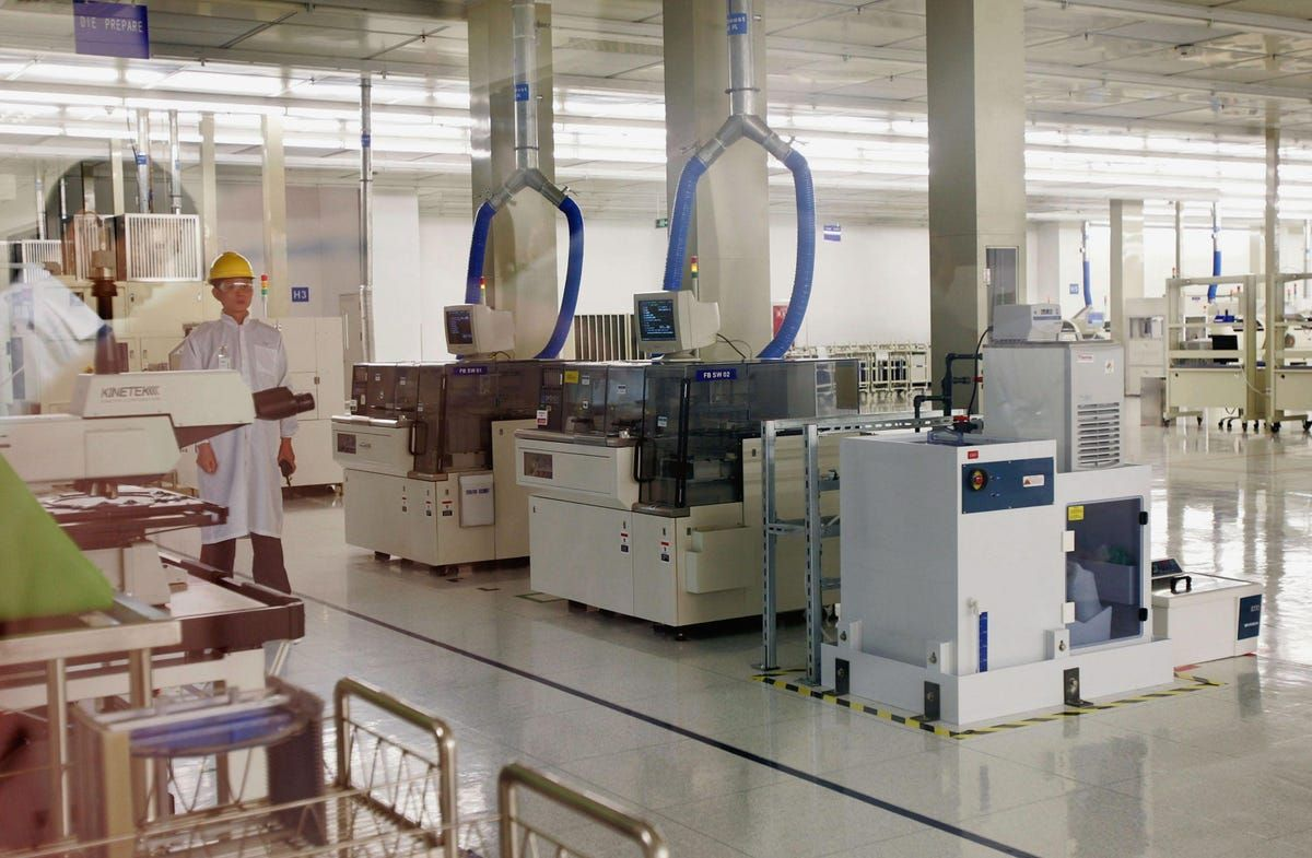
The economics behind next-generation semiconductor fabs has become one of the most important topics in the technology industry. Building an advanced semiconductor fabrication plant now requires enormous capital investment, highly specialized equipment, global supply chains, and years of planning. As artificial intelligence, high-performance computing, automotive electronics, and cloud infrastructure continue to expand, the economics behind next-generation semiconductor fabs increasingly determines which countries, suppliers, and manufacturers will lead the semiconductor industry over the next decade.
Unlike earlier manufacturing facilities, today’s semiconductor fabs operate at extreme technological limits. They rely on advanced lithography systems, ultra-pure materials, precision robotics, and highly automated production processes. Consequently, understanding the economics behind next-generation semiconductor fabs reveals why only a small number of organizations can afford to build and operate cutting-edge fabrication plants.
Why Next-Generation Semiconductor Fabs Cost So Much
The most advanced semiconductor fabrication facilities often require $20-40 billion or more before full-scale production begins. Several major factors contribute to these extraordinary costs.
Advanced Lithography Equipment
Extreme ultraviolet (EUV) lithography systems represent one of the largest expenses. A single EUV machine can cost hundreds of millions of dollars, and a leading-edge fab may require dozens of these systems. In addition, manufacturers must invest in installation, calibration, maintenance, and specialized infrastructure that supports these machines.
Cleanroom Infrastructure
Semiconductor manufacturing demands an environment that contains virtually no airborne particles. Therefore, next-generation fabs require massive cleanroom facilities with sophisticated filtration systems, climate control, vibration isolation, and contamination monitoring. Building and maintaining these environments significantly increases both construction and operating costs.
Specialized Manufacturing Equipment
Beyond lithography, fabs require deposition tools, etching systems, metrology equipment, ion implantation machines, wafer handling robotics, and advanced inspection platforms. Each production step adds another layer of capital expenditure.
As a result, the economics behind next-generation semiconductor fabs increasingly favors organizations with access to substantial financial resources and long-term investment horizons.
The Capital Expenditure Challenge
Semiconductor manufacturing is one of the most capital-intensive industries in the world. Unlike many manufacturing sectors, semiconductor fabs must continuously reinvest in new technology because process nodes evolve rapidly.
For example, a facility designed for one generation of manufacturing may require extensive upgrades only a few years later. Consequently, companies cannot simply build a fab and operate it unchanged for decades.
The capital expenditure cycle includes:
Facility construction
Equipment acquisition
Process development
Yield optimization
Capacity expansion
Technology upgrades
Therefore, semiconductor manufacturers must generate sufficient revenue not only to recover construction costs but also to fund future generations of manufacturing technology.
Economies of Scale in Semiconductor Manufacturing the Economics Behind Next-Generation
One reason semiconductor fabs continue growing larger is the powerful effect of economies of scale. Higher production volumes allow manufacturers to spread fixed costs across millions of chips.
Fixed Costs vs. Variable Costs
Most semiconductor fab expenses are fixed:
Building construction
Cleanroom infrastructure
Lithography equipment
Process development
Engineering staff
Variable costs, including wafers, chemicals, gases, and electricity, represent a smaller share of total expenses. Consequently, higher utilization rates dramatically improve profitability.
A fab operating at 95% capacity typically achieves much lower cost per chip than one operating at 60% capacity.
The AI Boom Is Reshaping Fab Economics
Artificial intelligence has transformed semiconductor demand. Modern AI accelerators require advanced process nodes, high-bandwidth memory, advanced packaging, and enormous wafer capacity.
This demand creates several economic effects:
Higher average selling prices
Long-term supply agreements
Capacity expansion investments
Increased equipment orders
Faster depreciation recovery
As AI workloads continue expanding, the economics behind next-generation semiconductor fabs increasingly depends on the ability to serve AI infrastructure markets.
Government Incentives and Industrial Policy of the Economics Behind Next-Generation
Governments around the world now view semiconductor manufacturing as a strategic industry. Therefore, many countries provide incentives to encourage domestic fabrication.
Common incentive programs include:
Direct construction subsidies
Tax credits
Research funding
Infrastructure support
Workforce development programs
Low-interest financing
These incentives significantly affect the economics behind next-generation semiconductor fabs by reducing the effective cost of new manufacturing facilities.
For example, semiconductor investment programs in the United States, Europe, Japan, and other regions aim to increase domestic production capacity and reduce supply-chain dependence.
Supply Chain Complexity and Financial Risk
A leading-edge semiconductor fab depends on a remarkably global supply chain.
Critical inputs include:
Silicon wafers
Photoresists
Specialty chemicals
Industrial gases
Precision optics
Semiconductor manufacturing equipment
Electronic materials
Packaging components
Any disruption in these supply chains can delay production and increase costs. Consequently, manufacturers often diversify suppliers, maintain inventory buffers, and invest in supply-chain resilience.
These protective measures improve reliability but also increase overall operating expenses.
Depreciation and Equipment Lifecycles the Economics Behind Next-Generation
Semiconductor equipment has a limited economic life. Manufacturers typically depreciate fabrication equipment over several years because technology advances quickly.
A simplified example illustrates the challenge:
Fab construction: $25 billion
Equipment investment: $15 billion
Total capital investment: $40 billion
If major equipment requires replacement after a relatively short period, annual depreciation expenses become substantial. Therefore, manufacturers must maintain high utilization rates and strong product demand to recover these investments efficiently.
Yield Rates: The Hidden Economic Driver
One of the most important economic variables in semiconductor manufacturing is yield.
Yield represents the percentage of chips on a wafer that function correctly after manufacturing.
For example:
70% yield means many chips become unusable.
95% yield dramatically lowers manufacturing cost per working chip.
Improving yield often requires years of process optimization, engineering expertise, statistical analysis, and advanced inspection technology.
Consequently, experienced manufacturers gain a significant economic advantage because they can produce more usable chips from the same wafer volume.
Advanced Packaging and Chiplet Economics
Modern semiconductor design increasingly relies on chiplet architectures rather than single monolithic dies.
Chiplets provide several economic advantages:
Better manufacturing yield
Modular product development
Reusable intellectual property
Faster design cycles
Flexible product configurations
Advanced packaging technologies, including 2.5D and 3D integration, enable manufacturers to combine multiple chiplets into a single high-performance package.
This shift changes the economics behind next-generation semiconductor fabs because value creation increasingly extends beyond wafer fabrication into advanced packaging and heterogeneous integration.
To understand how modular semiconductor design is transforming manufacturing strategy, read our detailed analysis of Open Chip Architectures and the Future of Modular Silicon.
The Economics of Capacity Expansion
Expanding semiconductor capacity is not as simple as adding another production line.
Manufacturers must consider:
Future demand forecasts
Equipment availability
Skilled labor supply
Utility infrastructure
Water consumption
Electricity requirements
Environmental regulations
Financing conditions
A new fab often requires three to five years before reaching meaningful production volumes. Therefore, companies must predict market conditions years in advance, creating significant financial risk.
Energy, Water, and Operating Costs the Economics Behind Next-Generation
Semiconductor fabs consume enormous quantities of electricity and ultra-pure water.
A large fabrication facility may require:
Hundreds of megawatts of electrical capacity
Millions of liters of purified water per day
Extensive wastewater treatment
Continuous climate control
High-reliability backup systems
Rising energy prices and water infrastructure costs increasingly influence fab location decisions and long-term operating economics.
Competition at Advanced Process Nodes
Only a limited number of manufacturers currently operate at the most advanced process nodes.
This concentration creates both advantages and risks.
Advantages
High pricing power
Strong customer demand
Premium product positioning
Long-term strategic partnerships
Risks
Massive capital requirements
Technology execution challenges
Equipment bottlenecks
Geopolitical exposure
Supply-chain dependence
As process nodes become more complex, the economics behind next-generation semiconductor fabs may become even more concentrated among manufacturers capable of sustaining continuous multi-billion-dollar investment cycles.
What Investors Watch Most Closely the Economics Behind Next-Generation
Investors evaluating semiconductor manufacturing companies typically focus on several key indicators:
Capital expenditure trends
Fab utilization rates
Gross margin performance
Yield improvements
Advanced node capacity
AI-related demand
Packaging capabilities
Government incentive support
Return on invested capital
Because semiconductor manufacturing requires such enormous upfront investment, small changes in utilization or pricing can significantly affect profitability.
The Long-Term Outlook
The economics behind next-generation semiconductor fabs will likely become even more important during the coming decade. Artificial intelligence, autonomous systems, robotics, cloud computing, advanced networking, and edge computing will continue increasing demand for sophisticated semiconductor manufacturing.
Several long-term trends appear especially significant:
Larger fabrication facilities
Greater automation
More advanced packaging
Increased chiplet adoption
Stronger government involvement
Higher energy efficiency requirements
Greater supply-chain regionalization
Although construction costs may continue rising, the strategic value of semiconductor manufacturing also continues increasing.
Final Thought
The economics behind next-generation semiconductor fabs extends far beyond the price of a factory. It involves capital allocation, technology leadership, supply-chain strategy, energy infrastructure, government policy, and global competition. Every advanced semiconductor fab represents a multi-decade financial commitment that can influence entire industries and national economies.
As AI accelerates semiconductor demand and manufacturing technology becomes more sophisticated, the economics behind next-generation semiconductor fabs will increasingly determine which regions lead future innovation. Understanding these economic forces helps explain why semiconductor manufacturing has become one of the most strategically important industries in the modern world.
For readers interested in broader semiconductor manufacturing trends, advanced packaging, and future chip architectures, explore additional hardware technology insights at Hashing Hardware.