
Introduction
Modern electronic devices require faster data processing, reliable communication, and efficient power delivery. From AI servers and networking equipment to industrial controllers and embedded systems, high-speed electronics depend on carefully designed printed circuit boards (PCBs).
However, achieving reliable performance involves more than selecting high-performance components. The internal structure of a PCB also plays an important role.
This is where PCB stackup design becomes essential.
A well-planned PCB stackup helps engineers manage signal integrity, impedance, electromagnetic interference, power distribution, and manufacturing requirements.
As data rates continue to increase, choosing the right number of layers, dielectric materials, copper thickness, and signal routing structure becomes increasingly important.
In this article, we explore how high-speed PCB stackup design works, which factors engineers should consider, and how to create a reliable multilayer PCB.
What Is PCB Stackup Design?
PCB stackup design refers to the arrangement of copper layers and insulating materials inside a printed circuit board.
A PCB can contain multiple signal layers, ground planes, power planes, and dielectric layers.
Each layer has a specific purpose. For example:
- Signal layers carry electrical signals between components.
- Ground planes provide reference paths for electrical signals.
- Power planes distribute power across the board.
- Dielectric layers separate conductive copper layers and provide electrical insulation.
The arrangement of these layers affects the electrical and mechanical performance of the PCB.
For simple electronic products, a two-layer PCB may be sufficient. However, high-speed and complex electronic systems often require four, six, eight, or more layers.
Why Is PCB Stackup Design Important?
A poorly planned stackup can create several electrical and manufacturing problems.
Here are the main reasons engineers should carefully plan the PCB layer structure.
1. Maintaining Signal Integrity
High-speed signals are sensitive to changes in trace geometry, impedance, and return-current paths.
An unsuitable layer arrangement can introduce signal reflections, crosstalk, and additional losses.
Placing critical signal traces close to an appropriate reference plane helps create a more controlled routing environment.
2. Controlling Impedance
Impedance is an important consideration in high-speed PCB design.
It depends on several factors, including:
- Trace width.
- Copper thickness.
- Dielectric thickness.
- Dielectric constant.
- Distance between signal and reference planes.
A properly defined stackup helps engineers achieve the target impedance required by high-speed interfaces.
3. Improving Power Distribution
Processors, memory devices, and other electronic components require stable power.
Dedicated power and ground planes can help distribute power across the board and support effective power integrity.
The placement and spacing of these planes should be considered alongside the board’s decoupling capacitor strategy.
4. Reducing Electromagnetic Interference
Ground planes provide reference paths and can help contain electromagnetic fields around signal routing.
A suitable layer arrangement can reduce unwanted coupling between different signals.
However, stackup design should work together with proper grounding, routing, shielding, and component placement.
5. Supporting Reliable Manufacturing
PCB stackup design also affects fabrication.
Layer count, board thickness, copper weight, dielectric materials, and via structures influence manufacturing complexity and cost.
Therefore, engineers should work with PCB manufacturers before finalizing the stackup.
Understanding the Different PCB Layers
Before designing a high-speed PCB, it is important to understand the purpose of each layer.
| Layer type | Main purpose |
|---|---|
| Signal layer | Carries electrical signals |
| Ground layer | Provides a reference and return-current path |
| Power layer | Distributes electrical power |
| Dielectric layer | Separates conductive layers |
| Solder mask | Protects exposed copper during assembly |
The number and arrangement of these layers depend on the application’s electrical, mechanical, and manufacturing requirements.
Common PCB Stackup Configurations
Different PCB applications require different layer arrangements.
1. Two-Layer PCB Stackup
A two-layer PCB contains copper on both sides of the board.
It is commonly used in simple electronic circuits, low-complexity embedded devices, and basic control systems.
Advantages:
- Lower manufacturing cost.
- Simple design process.
- Suitable for less complex circuits.
Limitations:
- Limited routing space.
- More difficult return-path management for complex high-speed signals.
- Less flexibility for separating power and ground structures.
2. Four-Layer PCB Stackup
A four-layer PCB provides additional routing and reference-plane options.
A common arrangement is:
- Layer 1: Signal
- Layer 2: Ground
- Layer 3: Power or ground
- Layer 4: Signal
This structure can provide useful reference planes for signal routing while keeping the board relatively compact.
Four-layer designs are common in embedded electronics, communication devices, and moderately complex digital systems.
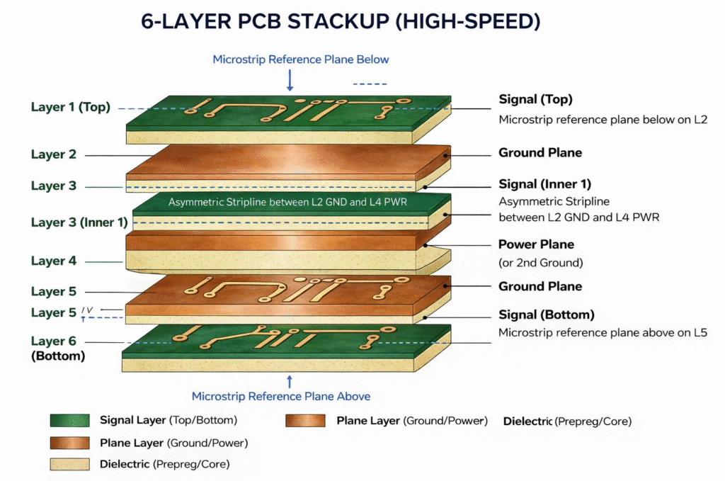
3. Six-Layer PCB Stackup
Six-layer PCBs provide additional routing flexibility.
One illustrative arrangement is:
- Layer 1: Signal
- Layer 2: Ground
- Layer 3: Signal
- Layer 4: Signal
- Layer 5: Power
- Layer 6: Signal
The actual arrangement should ensure that critical signals have suitable reference planes and that the board maintains appropriate electrical and mechanical balance.
4. Eight-Layer and Higher-Layer PCBs
High-density computing systems, networking equipment, and advanced electronic products may require eight or more layers.
These boards provide additional space for:
- High-speed signal routing.
- Power distribution.
- Ground reference planes.
- Dense component connections.
- Complex interface routing.
However, additional layers increase manufacturing complexity and can raise production costs.
Choosing the Right PCB Materials
Material selection is another important part of high-speed PCB stackup design.
The dielectric material between copper layers influences signal propagation and transmission losses.
Two important material properties are:
Dielectric Constant (Dk)
The dielectric constant describes how a material affects the electric field and signal propagation.
It influences the electrical characteristics of PCB transmission lines, including their impedance and propagation delay.
Designers should use material properties that match the intended operating frequencies and impedance requirements.
Dissipation Factor (Df)
The dissipation factor, also known as loss tangent, describes dielectric energy loss.
At higher frequencies, dielectric losses can become an important part of the total signal attenuation.
For demanding high-speed designs, engineers may evaluate low-loss materials such as specialized high-speed laminates.
Common PCB Materials
| Material | Typical applications |
|---|---|
| Standard FR-4 | General-purpose electronic circuits |
| High-speed FR-4 | Moderate-to-high-speed digital designs |
| Rogers laminates | RF and high-frequency applications |
| Megtron materials | High-speed communication and networking |
| Hybrid material construction | Designs balancing performance and cost |
The best material depends on frequency, insertion-loss requirements, operating environment, fabrication capabilities, and budget.
Using an expensive low-loss material everywhere is not always necessary. Hybrid stackups can use specialized materials for critical signal layers and conventional materials for other parts of the board.
Signal Routing Considerations in High-Speed PCB Design
Even with the correct stackup, poor routing can affect PCB performance.
Engineers should consider the following practices.
1. Maintain Continuous Reference Planes
High-speed signals need appropriate return-current paths.
Routing a critical signal across a split or gap in its reference plane can force return current to take a longer path.
This can increase loop inductance and electromagnetic interference.
Therefore, avoid unnecessary gaps beneath critical high-speed signal traces.
2. Control Trace Impedance
Trace dimensions should be calculated using the actual PCB stackup.
The trace width, copper thickness, dielectric height, and material properties all influence impedance.
Work with the PCB manufacturer to confirm achievable impedance tolerances.
3. Keep Differential Pairs Consistent
Many high-speed interfaces use differential signaling.
Differential pairs should maintain appropriate spacing, consistent geometry, and similar electrical path lengths.
Avoid unnecessary routing changes that create asymmetry between the two signals.
4. Minimize Unnecessary Layer Transitions
Every signal transition through a via can introduce an electrical discontinuity.
Use suitable via structures and avoid unnecessary transitions on critical high-speed signal paths.
For more information, read our guide on How Via Design Affects PCB Signal Integrity.
5. Separate Noisy and Sensitive Signals
Power switching circuits, clocks, and high-speed digital signals can create unwanted coupling.
Careful component placement and routing can help reduce interference between sensitive and noisy circuit sections.
Common PCB Stackup Design Mistakes to Avoid
Even experienced designers can encounter problems when stackup requirements are not considered early.
Some common mistakes include:
1. Choosing Layer Count Without Planning: Adding more layers does not automatically improve performance. Every layer should have a clear electrical or routing purpose.
2. Ignoring Dielectric Thickness: Incorrect dielectric spacing can affect impedance and signal performance.
3. Using Unsuitable Materials: Standard materials may not meet the loss requirements of demanding high-speed applications.
4. Poor Ground Plane Arrangement: Interrupted reference planes can create return-path problems.
5. Ignoring Manufacturing Limitations: A theoretically good stackup may be difficult or expensive for a manufacturer to produce.
6. Skipping Signal Integrity Analysis: High-speed designs should be evaluated before manufacturing rather than relying entirely on physical prototype testing.
A Practical Workflow for High-Speed PCB Stackup Design
A structured development process helps engineers reduce design errors.
Follow these steps:
- Understand the Application: Identify the required data rates, interfaces, operating frequencies, and performance targets.
- Select the Layer Count: Determine the required number of signal, power, and ground layers based on routing density and electrical requirements.
- Choose Suitable Materials: Evaluate dielectric constant, dissipation factor, copper characteristics, and material availability.
- Define the Stackup: Establish layer ordering, dielectric thickness, copper weight, and overall board thickness.
- Calculate Controlled Impedance: Work with the manufacturer to define suitable trace geometries and impedance requirements.
- Complete PCB Routing: Route critical signals with appropriate reference planes and return-current paths.
- Perform Simulation and Validation: Use signal integrity and power integrity analysis where appropriate.
- Review Manufacturing Requirements: Confirm the stackup, material availability, tolerances, and fabrication capabilities with the PCB manufacturer.
- Test the Prototype: Validate electrical performance under realistic operating conditions before production.
Where Is High-Speed PCB Stackup Design Used?
High-speed multilayer PCBs are used across many industries.
Some important applications include:
- AI servers and data center equipment.
- High-speed networking switches and routers.
- Telecommunications hardware.
- Automotive electronics.
- Industrial automation systems.
- Medical electronic equipment.
- Advanced embedded systems.
- High-performance computing platforms.
As electronic systems become faster and more compact, PCB stackup design will remain an important part of reliable hardware development.
Conclusion
High-speed PCB stackup design is an important part of modern electronic engineering.
The correct arrangement of signal layers, ground planes, power planes, and dielectric materials helps engineers manage impedance, signal integrity, power distribution, and electromagnetic interference.
However, there is no single stackup that works for every application.
Engineers must consider the operating frequency, routing density, material properties, manufacturing capabilities, and overall product requirements before finalizing the design.
By planning the stackup early and validating it through simulation and prototype testing, hardware teams can develop more reliable, efficient, and manufacturable PCB designs.
At HashingHardware, understanding PCB engineering fundamentals helps turn complex hardware requirements into practical and reliable electronic solutions.