
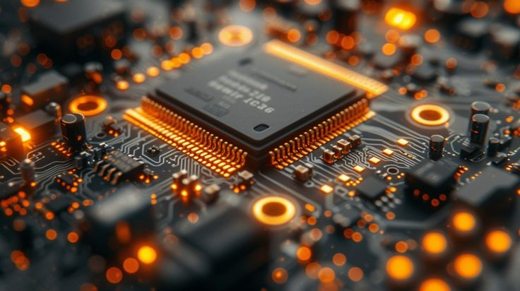
3D chip stacking is changing how processors get built. For decades, chips grew wider, not taller. That approach is running out of room. 3D chip stacking flips the model entirely. Instead of spreading transistors across a flat surface, engineers now stack chips on top of each other. Here is how this vertical shift works, and why it matters for AI hardware.
Why 3D Chip Stacking Became Necessary
Shrinking transistors keeps getting harder. Each new process node costs more and delivers smaller gains than the last. Consequently, chipmakers needed a second way to boost performance. 3D chip stacking offers exactly that.
The logic is simple. If you cannot make transistors much smaller, stack more of them vertically instead. TSMC put it plainly at its own technology symposium. If transistor scaling is slowing down, packaging becomes the new scaling engine. Therefore, 3D chip stacking is not a workaround. It is the industry’s next real lever for performance.
Face-to-Back vs Face-to-Face Stacking
Not all 3D chip stacking works the same way. Two distinct methods exist, and the difference matters enormously.
Face-to-back stacking was the first approach. Signals travel through vertical channels called through-silicon vias, or TSVs. Data crosses multiple metal layers before reaching its destination. That indirect path adds latency and burns extra power. Real-world designs using this method reach around 1,500 signal connections per square millimeter.
Face-to-face stacking takes a completely different route. It aligns two dies directly, connecting them through hybrid copper bonding instead of TSVs. Signals move in a straight, ultra-short vertical path. As a result, signal density jumps to roughly 14,000 connections per square millimeter, nearly ten times higher. Latency drops. Power efficiency improves. The stacked dies start behaving like a single chip instead of two separate ones.
TSMC’s SoIC Platform Leads the Charge 3D chip stacking
TSMC’s SoIC platform sits at the center of modern 3D chip stacking. The company’s roadmap tells a clear story of rapid progress. In 2023, TSMC offered a 9-micron bonding pitch. By 2025, that pitch tightened to 6 microns. TSMC now targets 4.5 microns by 2029.
Tighter pitches matter directly. A smaller pitch packs more vertical connections into the same space. That translates into more bandwidth and lower power use per bit. TSMC’s SVP Kevin Zhang confirmed the roadmap is accelerating, not slowing down, as newer process nodes gain stacking support faster than earlier generations did.
Apple has already put this to work. Its M5 series uses a variant called SoIC-mH, splitting CPU and GPU blocks across a larger horizontal mold. This spreads heat more evenly while still using vertical interconnects for unified memory. Meanwhile, Broadcom used TSMC’s face-to-face SoIC technology to help build Fujitsu’s Monaka processor, a 144-core data center CPU stacking compute chiplets directly on top of dedicated cache chiplets.
Intel and Samsung Take Their Own Paths
TSMC is not alone in this race. Intel developed Foveros, its own 3D stacking platform, first used at scale in Meteor Lake. The newer Foveros Direct technology adds direct copper-to-copper bonding, similar in spirit to TSMC’s face-to-face approach. Intel’s upcoming Clearwater Forest chips go a step further, adopting the UCIe standard so tiles from different foundries can mix and match within one package.
Samsung has its own answer too, called X-Cube. All three companies now treat 3D chip stacking as central to their roadmaps, not a side project. That shift alone signals how seriously the industry now takes vertical integration.
The Real Tradeoffs Nobody Skips
3D chip stacking is not free of challenges. Stacking high-performance logic directly on top of more logic creates serious heat problems. Broadcom and Fujitsu deliberately avoided logic-on-logic stacking in their Monaka design for exactly this reason. They stacked compute chiplets on cache instead, since cache generates far less heat.
Manufacturing complexity rises too. Broadcom, despite being an early adopter of face-to-face bonding, is still using a more conservative 9-micron pitch rather than TSMC’s newest 6-micron option. That caution says something important. Even sophisticated chipmakers move carefully when adopting bleeding-edge 3D stacking techniques.
Where 3D Chip Stacking Fits Alongside Faster Interconnects
3D chip stacking solves one half of a bigger problem. Getting more compute packed close together only helps if data can still move fast between chips and across a data center. That is exactly where optical interconnects come in, carrying data between racks and servers at speeds copper simply cannot match. For a closer look at how light-based connections are reshaping AI infrastructure, read our full guide to silicon photonics and the future of ultra-fast computing.
Final Thought
3D chip stacking marks a genuine turning point in how processors get designed. Shrinking transistors alone can no longer carry the industry forward on its own. TSMC, Intel, and Samsung are each racing to perfect vertical integration, tightening bonding pitches and refining face-to-face techniques year after year. The tradeoffs around heat and manufacturing complexity are real, and no company has fully solved them yet. Still, the direction is unmistakable. The next generation of AI and high-performance chips will not just get smaller. They will get taller.